IC Trays for Semiconductor and BGA Packaging
概要:
Review IC tray options for BGA and QFN devices. Request pocket drawings, material specifications, ESD evidence and samples for your handling process.
IC Trays for Semiconductor Handling and Packaging
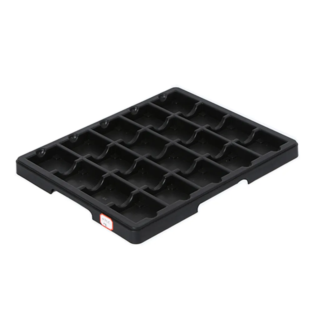
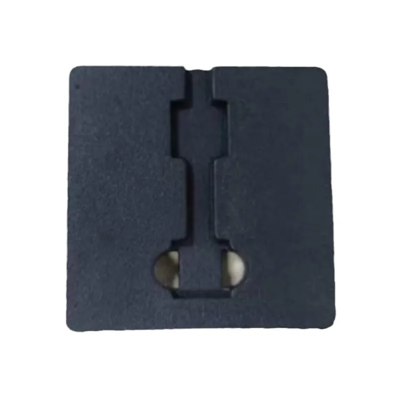
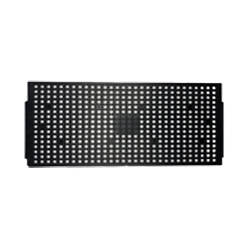
IC trays locate packaged semiconductor devices for controlled storage, inspection and handling. Select the pocket layout for the actual device package, permitted support areas and pickup process. SWESD’s catalogue on this page includes BGA and QFN tray options; confirm the current drawing and supplied configuration for the model you intend to purchase.
A tray’s appearance or an ESD description does not establish every required protective function. Ask for the relevant material and test evidence under your ESD control plan. Packaging used outside an ESD protected area may require discharge shielding as part of the complete package. See the EOS/ESD Association’s control principles for that distinction.
What to Confirm Before Ordering an IC Tray
- Device package drawing, pocket geometry, orientation and permitted contact surfaces.
- Tray outline, stacking interface and compatibility with the actual handling equipment.
- Material grade and the relevant electrical test method, conditions and results.
- Any required thermal exposure, its duration and the permitted supplier-defined conditions. Do not assume every device needs baking or every tray supports the same cycle.
- Sample acceptance, labeling, cleanliness, repeat supply and change notification requirements.
If JEDEC compatibility is required, specify the applicable current drawing or standard and request supporting evidence for the exact model. Confirming a tray outline does not by itself qualify the pocket, material or complete packaging arrangement for your device.
使用する tray drawing review guide, pocket tolerance checklist そして カスタムICトレイ見積依頼書(RFQ)ガイド to prepare a sample request. For the wider carrier range, browse SWESD ESD trays.
The catalogue figures below are product-listing information. Request the current supplier drawing, material specification, relevant test conditions and approved use limits before accepting a particular model for production. For a quotation, send your device drawing, handling route, quantity and evidence requirements through the SWESD inquiry page.
技術仕様書
Scroll the specification tables horizontally to compare all listed models.
| 商品名 | ICトレイ | ||||
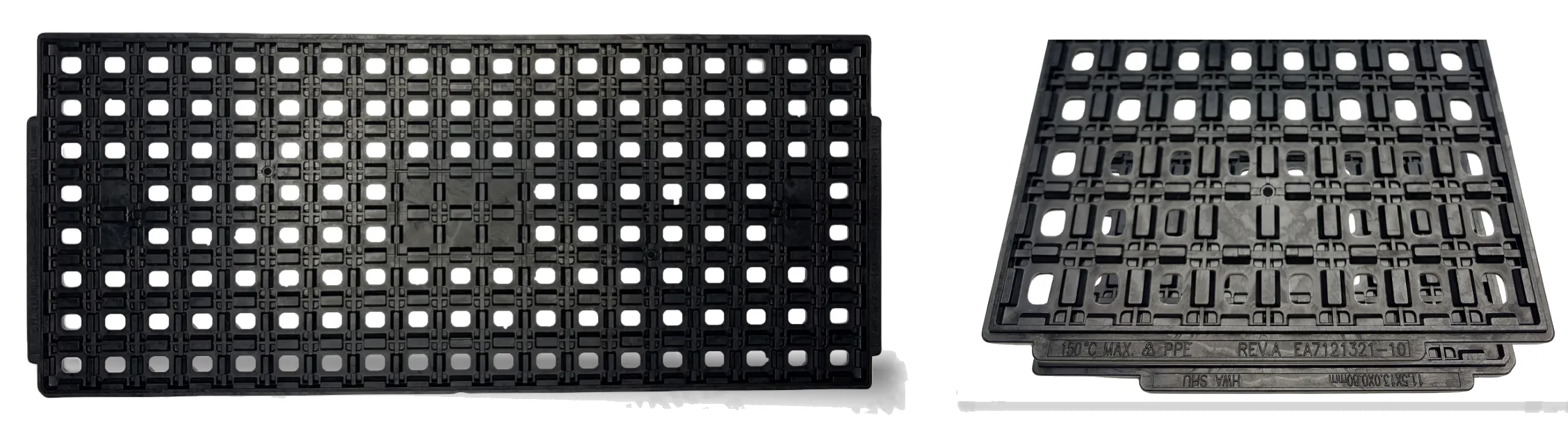
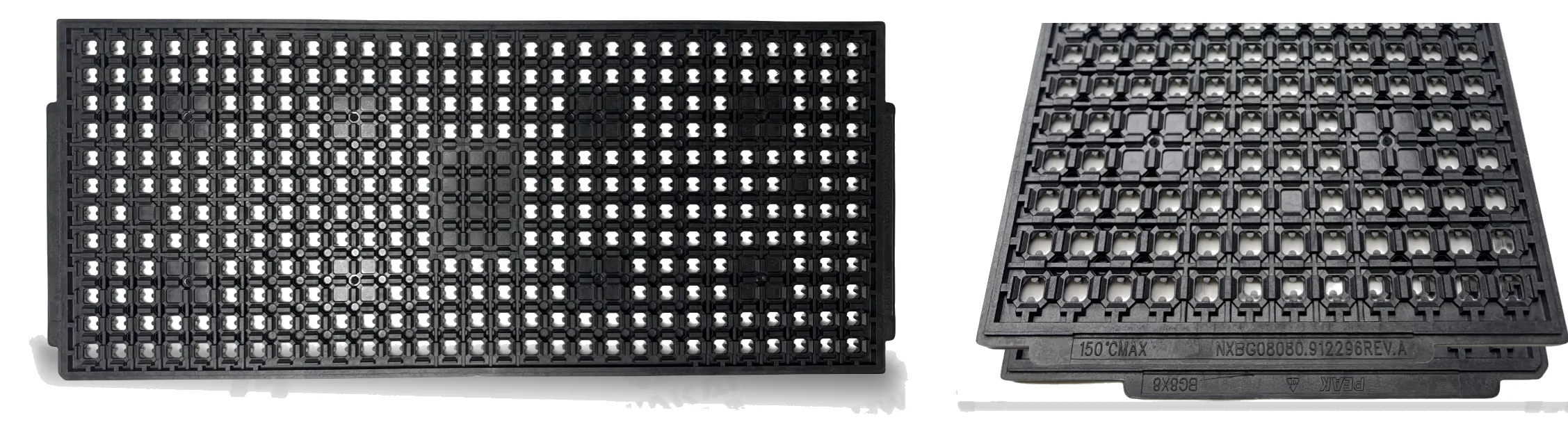
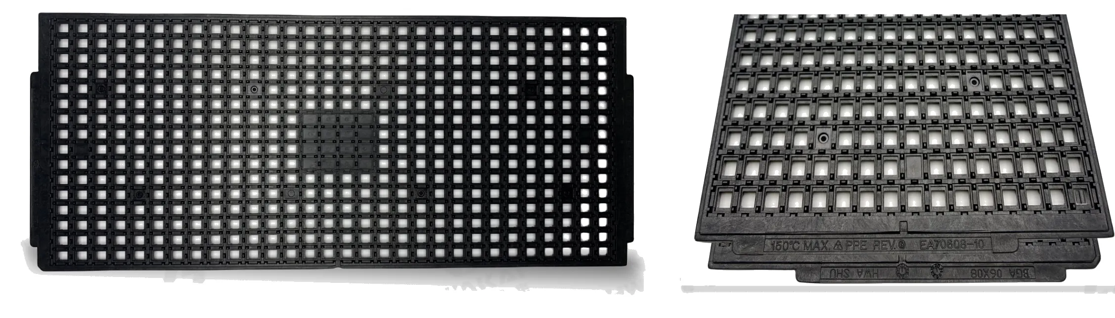
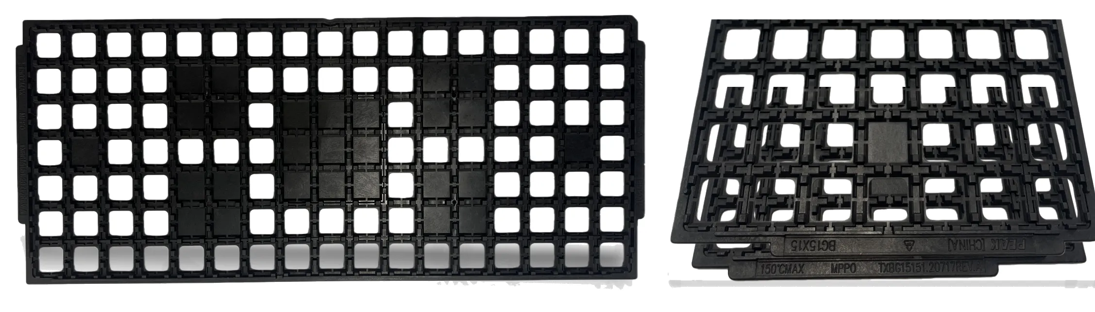
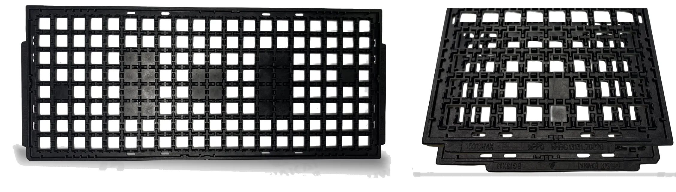
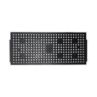
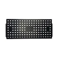
| 製品モデル | BGA6x8 | BGA8x8 | BGA11.5×13 | BGA13x13 | |
 |
 |
 |
 |
||
| 仕様パラメータ | ●Model | EA70608-10 | NXBG08080.912296REV.A | EA7121321-10 | NHBG13131.70820 |
| ●Tray cavity design | BGA | BGA | BGA | BGA | |
| ●Specifications | 6*8 | 8*8 | 11.5*13*0.8 | 13*13 | |
| ●Matrix | 16*30=480 | 12*29=348 | 8*19=152 | 8*20=160 | |
| ●Temperature MAX (℃) | 150 | 150 | 150 | 150 | |
| ●Surface Resistance | 10^5(Ω)~10^11(Ω) | 10^5(Ω)~10^11(Ω) | 10^5(Ω)~10^11(Ω) | 10^5(Ω)~10^11(Ω) | |
| ●Weight (g) | 138.5 | 162.4 | 125 | 110 | |
| 商品名 | ICトレイ | ||
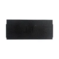
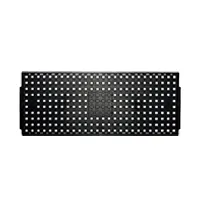
| 製品モデル | QFN5x5 | QFN7x7 | |
 |
 |
||
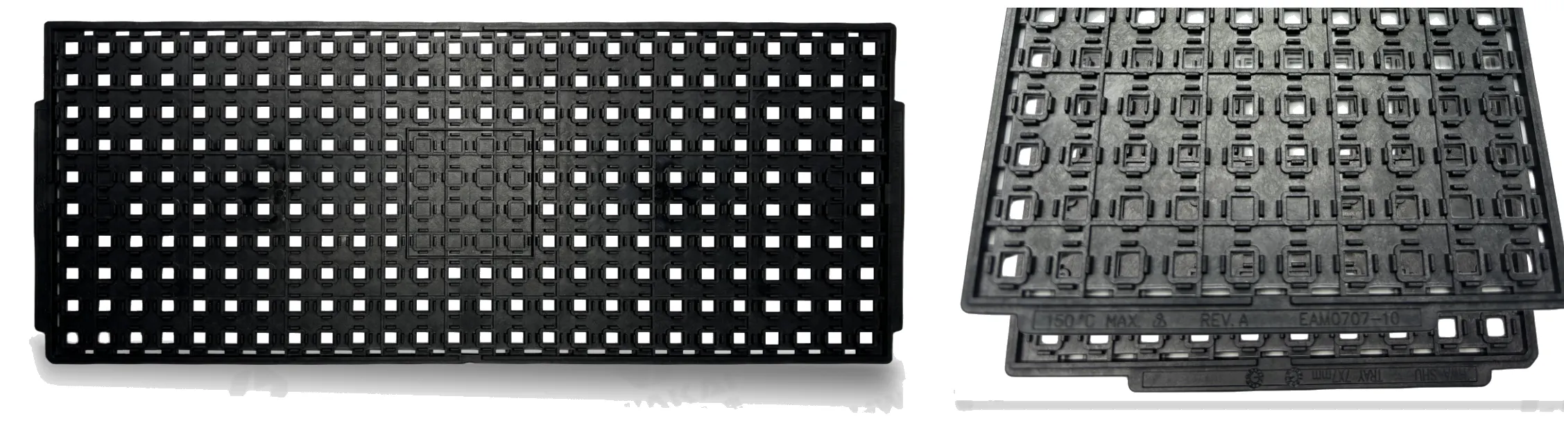
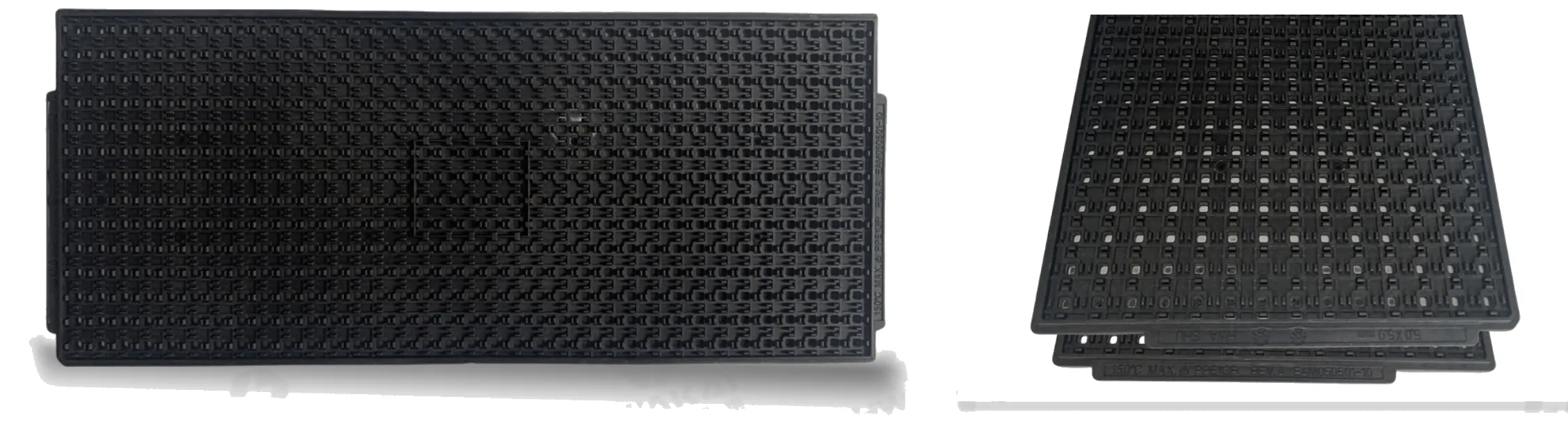
| 仕様パラメータ | ●Model | EAM050501-10 | EAM0707-10 |
| ●Tray cavity design | QFN | QFN | |
| ●Specifications | 5*5 | 7*7 | |
| ●Matrix | 14*35=490 | 10*26=260 | |
| ●Temperature MAX (℃) | 150 | 150 | |
| ●Surface Resistance | 10^5(Ω)~10^11(Ω) | 10^4(Ω)~10^11(Ω) | |
| ●Weight (g) | 183.9 | 148 | |
世界最高水準のESD製造能力
三威から調達する場合、業界をリードするOEM/ODMメーカーと直接提携することになります。当社は最先端の 7万m²超の一貫生産拠点 浙江省楽清中心工業団地において、独自の材料配合から最終的な高精度製品の成形に至るまで、すべての工程を自社で管理しています。.
統合されたスケール
7万平方メートル超の最新鋭の工場基盤に、高負荷・高精度の射出成形機を備え、安定したリードタイムで大口の卸売注文に対応します。.
フルチェーン制御
独自開発の制電材料の研究開発から、構造金型の設計、自動化製造、迅速なグローバル物流まで、すべてを自社内で一貫して管理しています。.
厳格な検査
厳格な原材料検査と、生産ラインにおける多点表面抵抗値 測定を組み合わせることで、100%が国際的なESD基準ガイドラインに準拠していることが保証されます。.
帯電防止 製品とソリューション
製造および運用のライフサイクル全体にわたり、包括的な静電気保護を提供します。.
実装機
自動ライン用帯電防止コレクションボックスおよびラック.

保管と物流
台車、棚、箱、トレイ、および部品容器.

ワークステーションとPPE
制電椅子、マット、リストストラップ、および個人用保護具。.
カスタム開発
カスタム金型の開発と特殊な制電材料。.
当社のOEM/ODMの強み

先進R&D・材料イノベーション
国家発明特許を取得し、耐熱温度は200℃に達する自社開発の制電材料。私たちは成形するだけでなく、コンパウンド(配合)から手掛けます。.

本格生産能力
安定した効率的な供給を実現するため、射出成形、造粒、および関連する加工システムを完備した30,000㎡の工場。.

一貫したフルカスタム
材料の固有抵抗、色、サイズ、ロゴ、パッケージ、認証は、IEC61340-5-1、ANSI/ESD S20.20、または軍用規格に適合するようにカスタマイズ可能です。.

品質保証・グローバルコンプライアンス認証
“三維社は半導体組立ライン向けに、カスタム仕様の高耐熱クリーンナチュラルカラートレイの開発に成功しました。これにより輸入品の代替を実現し、優れたESD安全性を確保するとともに、クリーンルームの高い清浄度要件を満たしました。”
世界的なフォーチュン500の業界リーダーから信頼されています
当社独自のESDソリューションは、以下をはじめとする世界のエリート生産施設に導入されています。 インテル、モトローラ、シーメンス、IBM、パナソニック、ノキア、デル。.
カスタムサイズや大口卸売価格をお探しですか?
三維は、自社内の強力なR&Dチームを基盤とし、お客様の特定のSMT生産ラインや倉庫レイアウトに合わせた完全なOEM/ODMオプションを提供します。カスタム金型、色分け、または統合された5Sストレージコンサルティングについて、今すぐ専門家にお問い合わせください。.
よくある質問 (FAQ)
1. What is an IC tray?
It’s basically a plastic tray that holds semiconductor chips during manufacturing, testing, shipping, and storage. They’re specially made to be ESD‑safe so static doesn’t fry the chips. Most of them follow standard sizes so they work with automated handling equipment.
2. What are the materials used in IC packaging?
That’s a whole “package” of stuff – you’ve got the molding compound (usually epoxy resin), a substrate (organic or ceramic), lead frames, die attach adhesives, bonding wires, and solder balls. All these materials work together to protect the chip, connect it to the circuit, and help keep it cool.
3. What material are ice trays made of?
Ice trays for your freezer are a totally different story – they’re all about food safety. The most common are food‑grade polypropylene (PP) and silicone. Silicone’s nice because it’s flexible and makes popping out the ice cubes super easy.
4. What is the standard tray size?
When people say “standard tray,” they usually mean the JEDEC size – that’s 12.7 x 5.35 inches, or about 322.6 x 136 mm. Thickness can be either 0.25 inches (thin) or 0.40 inches (thick). There’s also a common 320mm x 240mm size used internationally.
5. What is a JEDEC tray?
It’s a tray that meets the specs set by JEDEC – the group that writes standards for the semiconductor industry. Think of it as a universal container for chips (like BGA or QFP packages) so that trays from different manufacturers all fit the same machines and processes.
6. What is the tolerance of JEDEC trays?
They’re made to pretty tight tolerances to make sure chips sit exactly right. For example, the dimension accuracy is often around ±0.15 mm, and the overall flatness is kept within about 0.76 mm. That said, the exact numbers can vary a bit between suppliers – always check the data sheet.
7. What is the JEDEC standard?
JEDEC is basically the rule‑maker for the microelectronics world. They publish standards for everything from memory chips (like DDR5) to how parts are packaged and tested. It’s the common language that makes sure chips from different companies can work together.
8. What is the difference between JEDEC and IPC?
Think of it this way: JEDEC focuses on the chip itself – its electrical specs, physical dimensions, and testing. IPC, on the other hand, deals with the circuit board and assembly – how PCBs are designed, manufactured, and soldered. So JEDEC is about the silicon, IPC is about the board.