IC Trays for Semiconductor and BGA Packaging
Przegląd:
Review IC tray options for BGA and QFN devices. Request pocket drawings, material specifications, ESD evidence and samples for your handling process.
IC Trays for Semiconductor Handling and Packaging
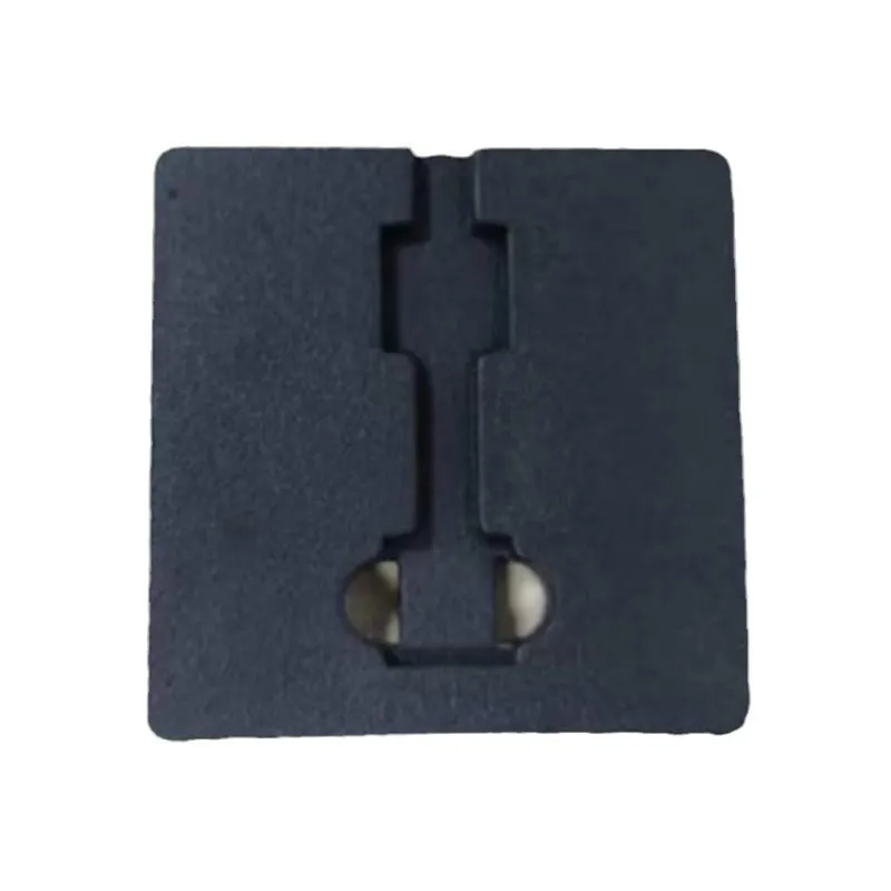
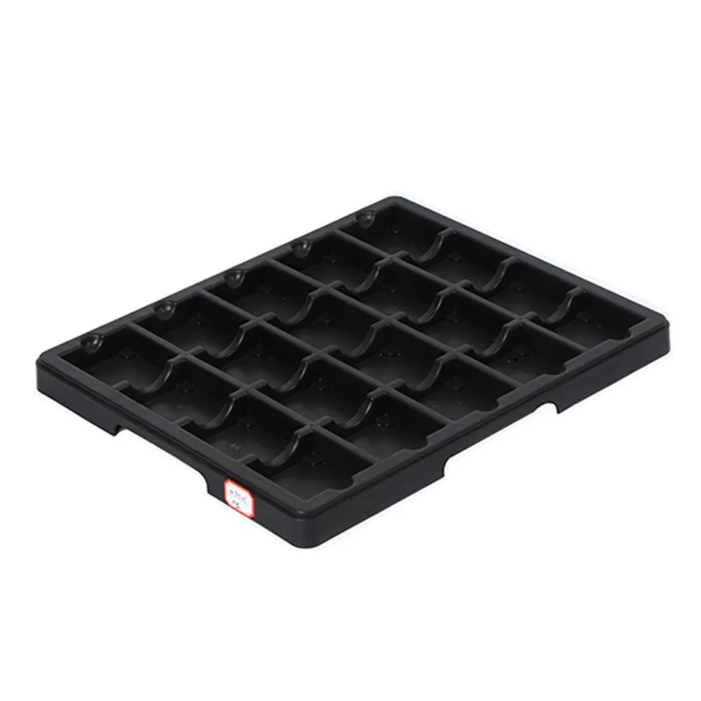
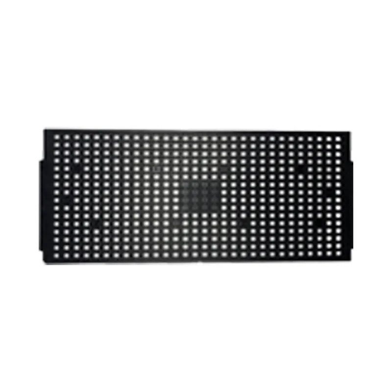
IC trays locate packaged semiconductor devices for controlled storage, inspection and handling. Select the pocket layout for the actual device package, permitted support areas and pickup process. SWESD’s catalogue on this page includes BGA and QFN tray options; confirm the current drawing and supplied configuration for the model you intend to purchase.
A tray’s appearance or an ESD description does not establish every required protective function. Ask for the relevant material and test evidence under your ESD control plan. Packaging used outside an ESD protected area may require discharge shielding as part of the complete package. See the EOS/ESD Association’s control principles for that distinction.
What to Confirm Before Ordering an IC Tray
- Device package drawing, pocket geometry, orientation and permitted contact surfaces.
- Tray outline, stacking interface and compatibility with the actual handling equipment.
- Material grade and the relevant electrical test method, conditions and results.
- Any required thermal exposure, its duration and the permitted supplier-defined conditions. Do not assume every device needs baking or every tray supports the same cycle.
- Sample acceptance, labeling, cleanliness, repeat supply and change notification requirements.
If JEDEC compatibility is required, specify the applicable current drawing or standard and request supporting evidence for the exact model. Confirming a tray outline does not by itself qualify the pocket, material or complete packaging arrangement for your device.
Użyj tray drawing review guide, pocket tolerance checklist i Przewodnik zapytania ofertowego (RFQ) dotyczący niestandardowych tac na układy scalone to prepare a sample request. For the wider carrier range, browse SWESD ESD trays.
The catalogue figures below are product-listing information. Request the current supplier drawing, material specification, relevant test conditions and approved use limits before accepting a particular model for production. For a quotation, send your device drawing, handling route, quantity and evidence requirements through the SWESD inquiry page.
Specyfikacja techniczna
Scroll the specification tables horizontally to compare all listed models.
| Nazwa produktu | tacka IC | ||||
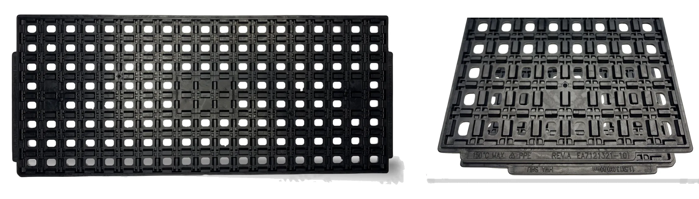
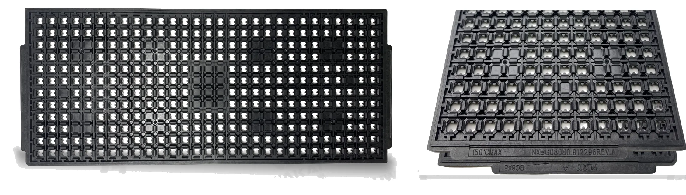
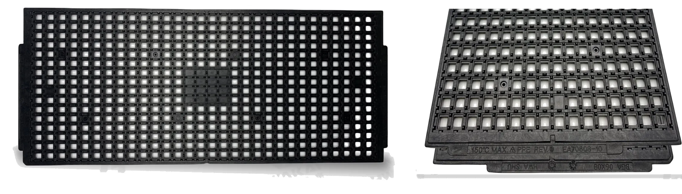
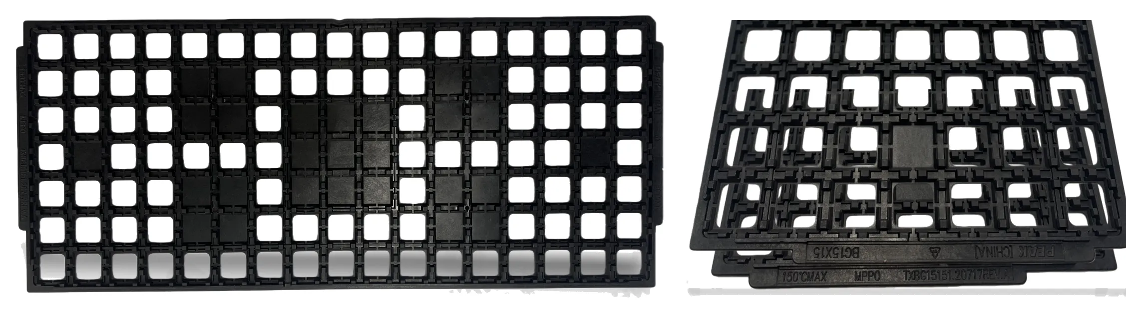
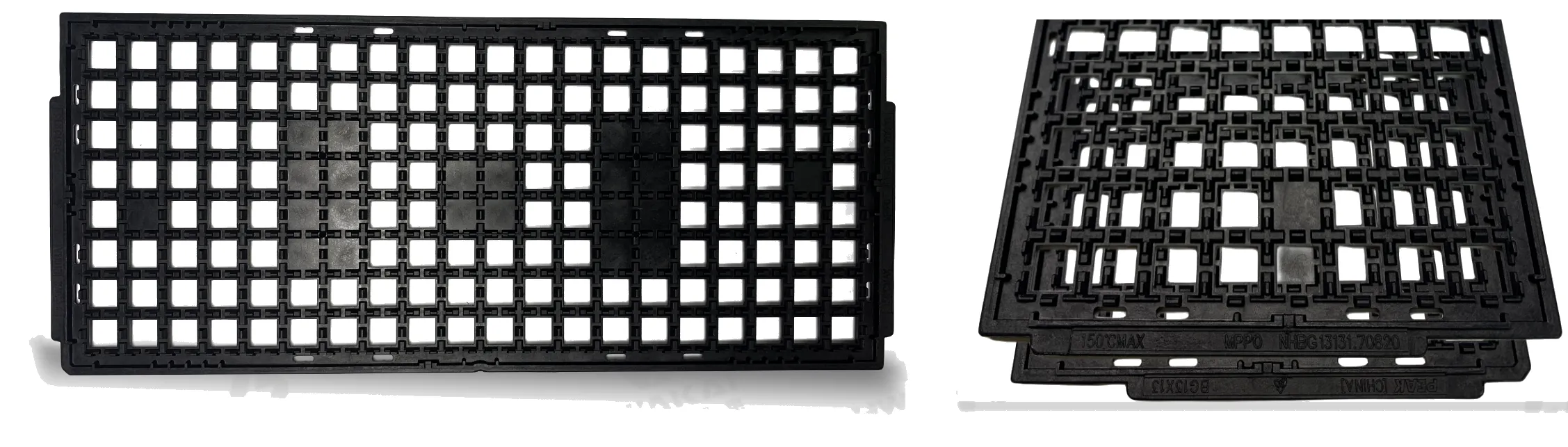
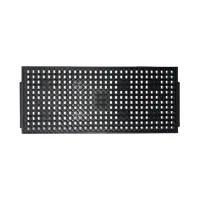
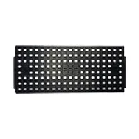
| Model produktu | BGA6x8 | BGA8x8 | BGA11.5×13 | BGA13x13 | |
 |
 |
 |
 |
||
| Parametry specyfikacji | ●Model | EA70608-10 | NXBG08080.912296REV.A | EA7121321-10 | NHBG13131.70820 |
| ●Tray cavity design | BGA | BGA | BGA | BGA | |
| ●Specifications | 6*8 | 8*8 | 11.5*13*0.8 | 13*13 | |
| ●Matrix | 16*30=480 | 12*29=348 | 8*19=152 | 8*20=160 | |
| ●Temperature MAX (℃) | 150 | 150 | 150 | 150 | |
| ●Surface Resistance | 10^5(Ω)~10^11(Ω) | 10^5(Ω)~10^11(Ω) | 10^5(Ω)~10^11(Ω) | 10^5(Ω)~10^11(Ω) | |
| ●Weight (g) | 138.5 | 162.4 | 125 | 110 | |
| Nazwa produktu | tacka IC | ||
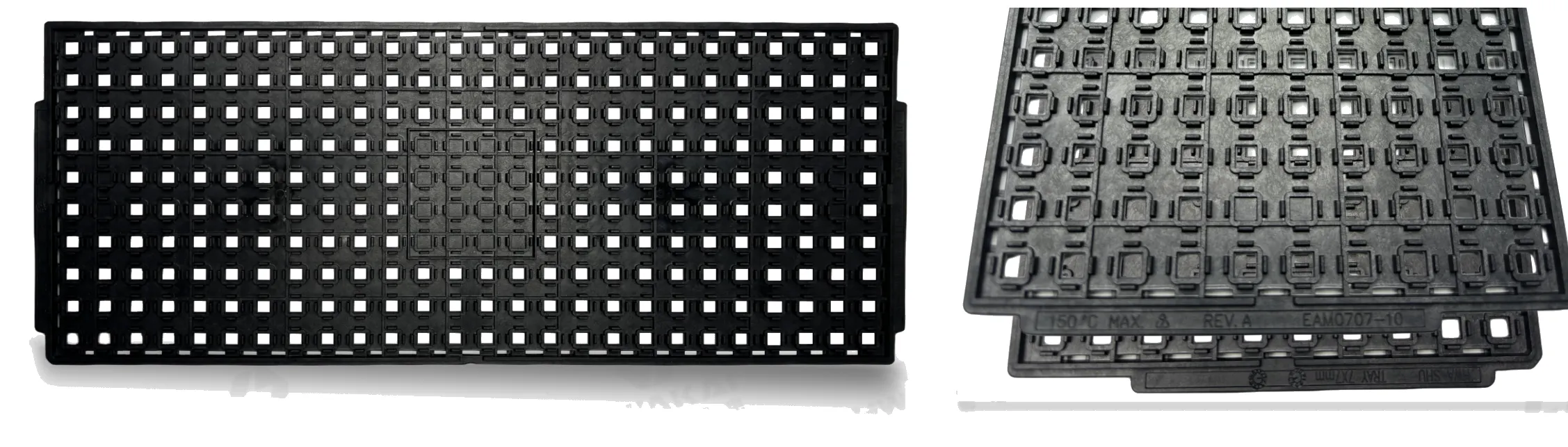
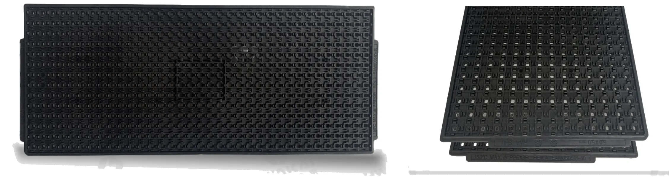
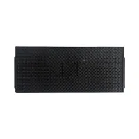
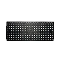
| Model produktu | QFN5x5 | QFN7x7 | |
 |
 |
||
| Parametry specyfikacji | ●Model | EAM050501-10 | EAM0707-10 |
| ●Tray cavity design | QFN | QFN | |
| ●Specifications | 5*5 | 7*7 | |
| ●Matrix | 14*35=490 | 10*26=260 | |
| ●Temperature MAX (℃) | 150 | 150 | |
| ●Surface Resistance | 10^5(Ω)~10^11(Ω) | 10^4(Ω)~10^11(Ω) | |
| ●Weight (g) | 183.9 | 148 | |
Światowej klasy potencjał produkcyjny ESD
Wybierając współpracę z Sanwei, partnerujesz bezpośrednio z wiodącym w branży producentem OEM/ODM. Posiadamy nowoczesne Zintegrowany zakład produkcyjny o powierzchni ponad 70 000 m² w Centralnym Parku Przemysłowym Yueqing w prowincji Zhejiang, zarządzając każdym pojedynczym procesem, od opracowania własnych formulacji materiałowych po ostateczne formowanie produktów o wysokiej precyzji.
Zintegrowana skala
Ponad 70 000 m² nowoczesnego zakładu wyposażonego w wytrzymałe, precyzyjne wtryskarki do obsługi hurtowych zamówień masowych z zachowaniem stabilnych terminów realizacji.
Kontrola całego łańcucha
Pełna kontrola wewnętrzna obejmująca badania i rozwój własnych materiałów antyelektrostatycznych, projektowanie form konstrukcyjnych, zautomatyzowaną produkcję oraz szybką globalną logistykę dostaw.
Rygorystyczna inspekcja
Rygorystyczne badania surowców w połączeniu z wielopunktowym pomiarem rezystywności powierzchniowej na linii produkcyjnej gwarantują zgodność modelu 100% z wytycznymi międzynarodowych norm dotyczących ochrony przed wyładowaniami elektrostatycznymi (ESD).
Antystatyczny Produkty i rozwiązania
Zapewnienie kompleksowej ochrony elektrostatycznej w całym cyklu produkcyjnym i operacyjnym.
Sprzęt SMT
Antystatyczne pojemniki zbiorcze i stojaki do linii zautomatyzowanych.

Magazynowanie i logistyka
Wózki technologiczne, półki, skrzynie, tace i pojemniki na komponenty.

Stanowisko robocze i ŚOI
Antystatyczne krzesła, maty, paski na nadgarstek oraz ochrona osobista.
Wdrożenia dedykowane
Rozwój niestandardowych form oraz specjalne materiały antystatyczne.
NASZE ZALETY OEM/ODM

Zaawansowane prace B+R i innowacje materiałowe
Własne materiały antystatyczne opracowane wewnątrz firmy, objęte krajowymi patentami na wynalazki i odporne na temperaturę do 200℃. My nie tylko formujemy – my tworzymy związki chemiczne.

Pełnomocna zdolność produkcyjna
Fabryka o powierzchni 30 000 m² z kompletinymi systemami formowania wtryskowego, granulacji i przetwarzania wspomagającego dla zapewnienia stabilnych i wydajnych dostaw.

Kompleksowa personalizacja
Rezystywność materiału, kolor, rozmiar, logo, opakowanie i certyfikaty – możliwość dostosowania do norm IEC61340-5-1, ANSI/ESD S20.20 lub norm wojskowych.

Certyfikowana jakość i globalna zgodność z przepisami
“Firma Sanwei z powodzeniem opracowała niestandardowe, odporne na wysokie temperatury tace o czystym, naturalnym kolorze dla naszej linii montażowej półprzewodników, zastępując produkty importowane, zapewniając doskonałe bezpieczeństwo ESD i spełniając wysokie wymagania dotyczące czystości warsztatu.”
ZAUFALI MIĘDZYNARODOWYM LIDEROM RYNKOWYM Z LISTY FORTUNE 500
Nasze autorskie rozwiązania ESD są wdrażane w elitarnych zakładach produkcyjnych na całym świecie, w tym: Intel, Motorola, Siemens, IBM, Panasonic, Nokia i Dell.
Szukasz niestandardowych rozmiarów lub hurtowych cen?
Wspierani przez nasz silny, wewnętrzny zespół Badawczo-Rozwojowy (R&D), oferujemy kompleksowe opcje OEM/ODM dostosowane do Twoich konkretnych linii produkcyjnych SMT lub układu magazynu. Skontaktuj się z naszymi specjalistami już dziś w sprawie niestandardowych form, kodowania kolorami lub zintegrowanego doradztwa w zakresie magazynowania 5S.
Często zadawane pytania (FAQ)
1. What is an IC tray?
It’s basically a plastic tray that holds semiconductor chips during manufacturing, testing, shipping, and storage. They’re specially made to be ESD‑safe so static doesn’t fry the chips. Most of them follow standard sizes so they work with automated handling equipment.
2. What are the materials used in IC packaging?
That’s a whole “package” of stuff – you’ve got the molding compound (usually epoxy resin), a substrate (organic or ceramic), lead frames, die attach adhesives, bonding wires, and solder balls. All these materials work together to protect the chip, connect it to the circuit, and help keep it cool.
3. What material are ice trays made of?
Ice trays for your freezer are a totally different story – they’re all about food safety. The most common are food‑grade polypropylene (PP) and silicone. Silicone’s nice because it’s flexible and makes popping out the ice cubes super easy.
4. What is the standard tray size?
When people say “standard tray,” they usually mean the JEDEC size – that’s 12.7 x 5.35 inches, or about 322.6 x 136 mm. Thickness can be either 0.25 inches (thin) or 0.40 inches (thick). There’s also a common 320mm x 240mm size used internationally.
5. What is a JEDEC tray?
It’s a tray that meets the specs set by JEDEC – the group that writes standards for the semiconductor industry. Think of it as a universal container for chips (like BGA or QFP packages) so that trays from different manufacturers all fit the same machines and processes.
6. What is the tolerance of JEDEC trays?
They’re made to pretty tight tolerances to make sure chips sit exactly right. For example, the dimension accuracy is often around ±0.15 mm, and the overall flatness is kept within about 0.76 mm. That said, the exact numbers can vary a bit between suppliers – always check the data sheet.
7. What is the JEDEC standard?
JEDEC is basically the rule‑maker for the microelectronics world. They publish standards for everything from memory chips (like DDR5) to how parts are packaged and tested. It’s the common language that makes sure chips from different companies can work together.
8. What is the difference between JEDEC and IPC?
Think of it this way: JEDEC focuses on the chip itself – its electrical specs, physical dimensions, and testing. IPC, on the other hand, deals with the circuit board and assembly – how PCBs are designed, manufactured, and soldered. So JEDEC is about the silicon, IPC is about the board.