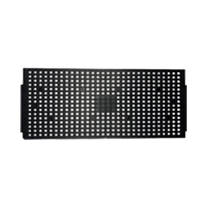
IC Trays for Semiconductor and BGA Packaging
Ikhtisar:
Review IC tray options for BGA and QFN devices. Request pocket drawings, material specifications, ESD evidence and samples for your handling process.
IC Trays for Semiconductor Handling and Packaging
IC trays locate packaged semiconductor devices for controlled storage, inspection and handling. Select the pocket layout for the actual device package, permitted support areas and pickup process. SWESD’s catalogue on this page includes BGA and QFN tray options; confirm the current drawing and supplied configuration for the model you intend to purchase.
A tray’s appearance or an ESD description does not establish every required protective function. Ask for the relevant material and test evidence under your ESD control plan. Packaging used outside an ESD protected area may require discharge shielding as part of the complete package. See the EOS/ESD Association’s control principles for that distinction.
What to Confirm Before Ordering an IC Tray
- Device package drawing, pocket geometry, orientation and permitted contact surfaces.
- Tray outline, stacking interface and compatibility with the actual handling equipment.
- Material grade and the relevant electrical test method, conditions and results.
- Any required thermal exposure, its duration and the permitted supplier-defined conditions. Do not assume every device needs baking or every tray supports the same cycle.
- Sample acceptance, labeling, cleanliness, repeat supply and change notification requirements.
If JEDEC compatibility is required, specify the applicable current drawing or standard and request supporting evidence for the exact model. Confirming a tray outline does not by itself qualify the pocket, material or complete packaging arrangement for your device.
Gunakan tray drawing review guide, pocket tolerance checklist dan Panduan RFQ baki IC kustom to prepare a sample request. For the wider carrier range, browse SWESD ESD trays.
The catalogue figures below are product-listing information. Request the current supplier drawing, material specification, relevant test conditions and approved use limits before accepting a particular model for production. For a quotation, send your device drawing, handling route, quantity and evidence requirements through the SWESD inquiry page.
Spesifikasi Teknis
Scroll the specification tables horizontally to compare all listed models.
| Product name | Baki IC | ||||
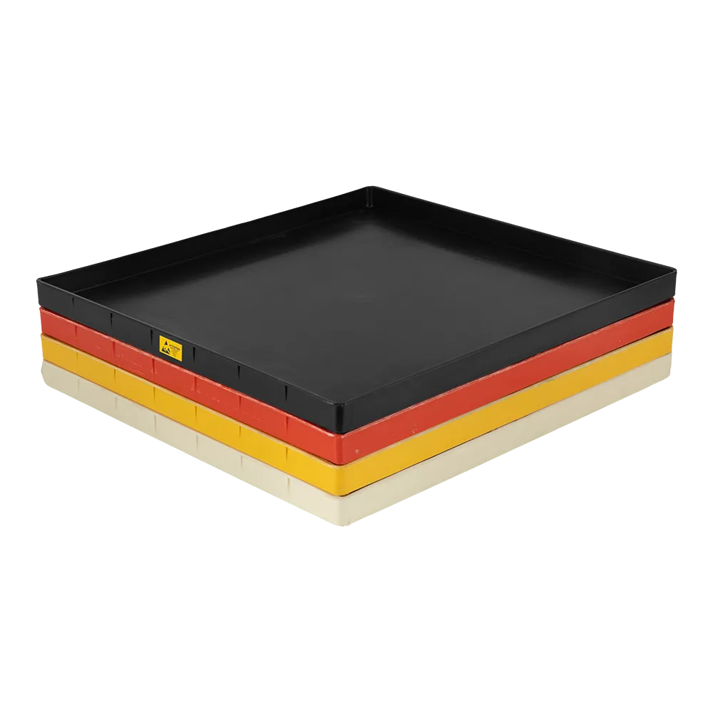
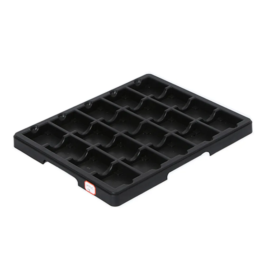
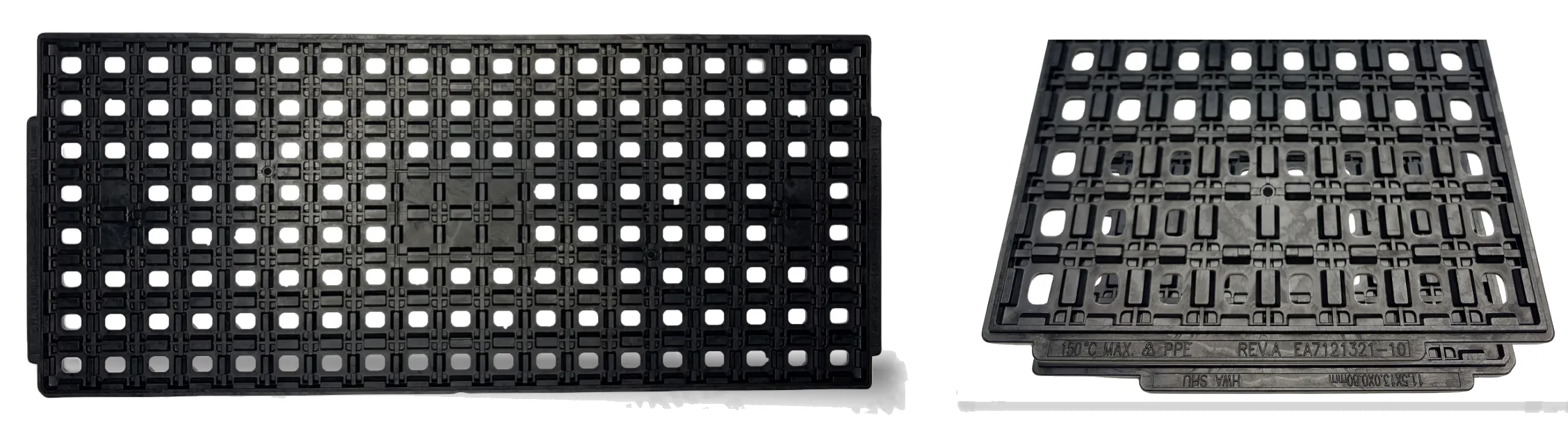
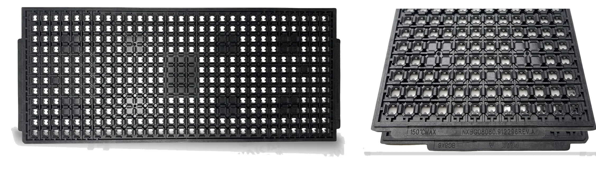
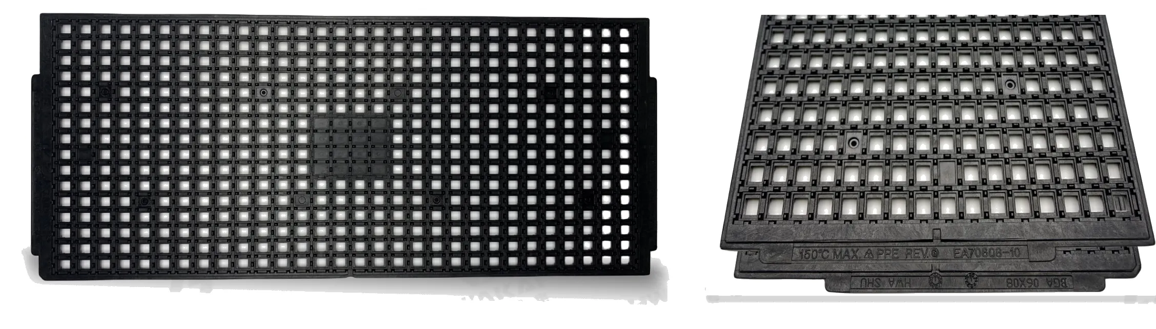
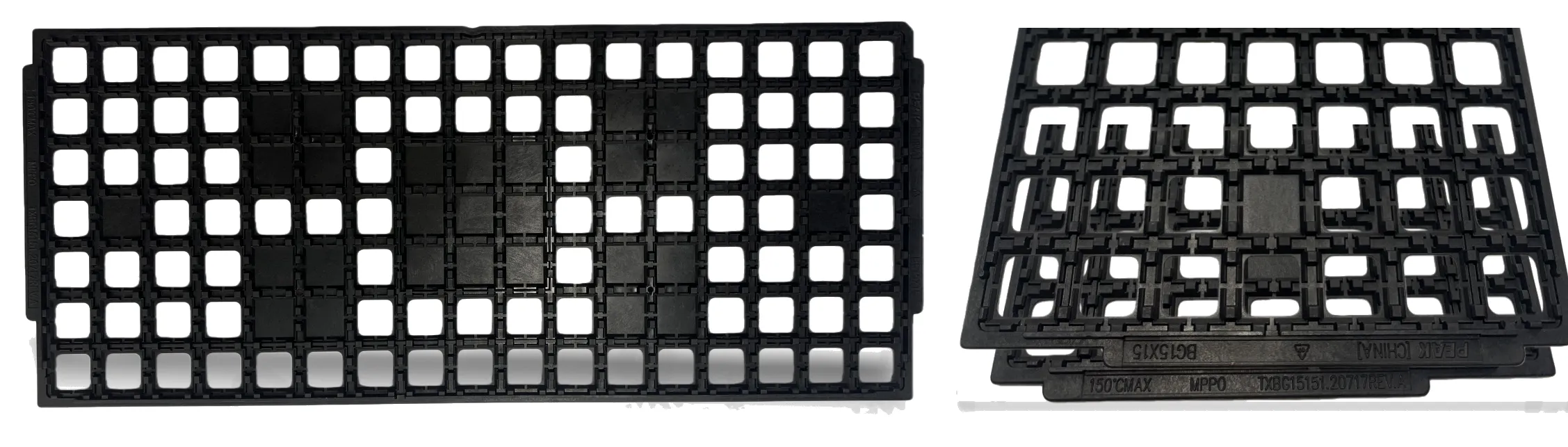
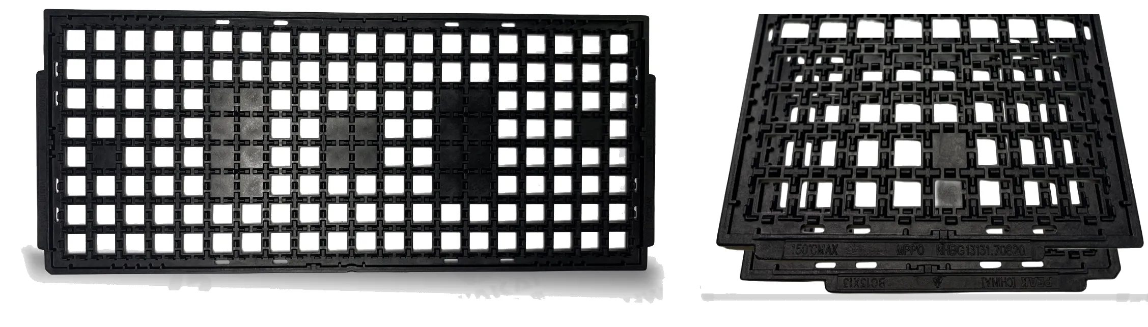
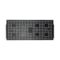
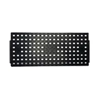
| Product model | BGA6x8 | BGA8x8 | BGA11.5×13 | BGA13x13 | |
 |
 |
 |
 |
||
| Specification parameters | ●Model | EA70608-10 | NXBG08080.912296REV.A | EA7121321-10 | NHBG13131.70820 |
| ●Tray cavity design | BGA | BGA | BGA | BGA | |
| ●Specifications | 6*8 | 8*8 | 11.5*13*0.8 | 13*13 | |
| ●Matrix | 16*30=480 | 12*29=348 | 8*19=152 | 8*20=160 | |
| ●Temperature MAX (℃) | 150 | 150 | 150 | 150 | |
| ●Surface Resistance | 10^5(Ω)~10^11(Ω) | 10^5(Ω)~10^11(Ω) | 10^5(Ω)~10^11(Ω) | 10^5(Ω)~10^11(Ω) | |
| ●Weight (g) | 138.5 | 162.4 | 125 | 110 | |
| Product name | Baki IC | ||
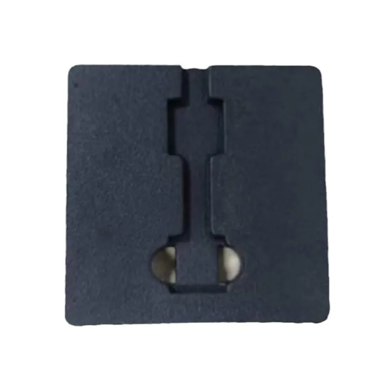
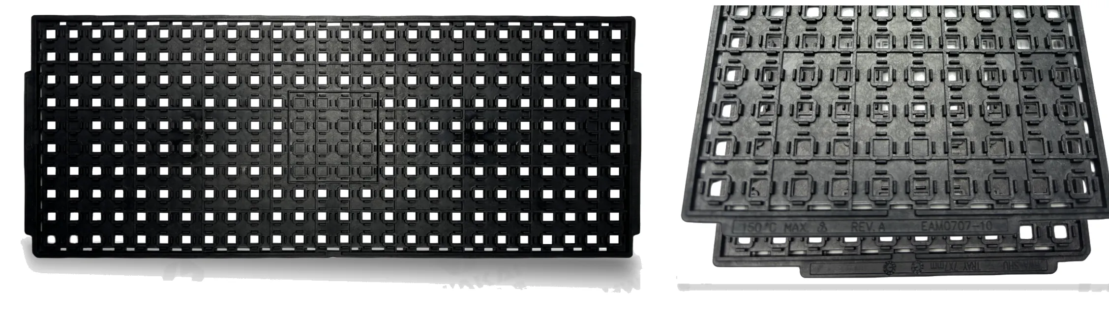
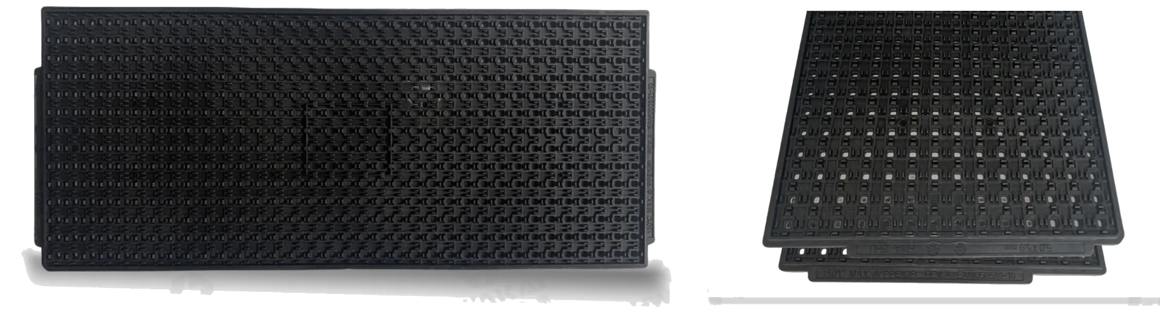
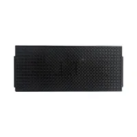
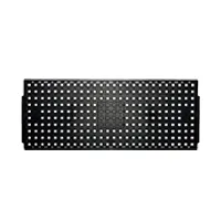
| Product model | QFN5x5 | QFN7x7 | |
 |
 |
||
| Specification parameters | ●Model | EAM050501-10 | EAM0707-10 |
| ●Tray cavity design | QFN | QFN | |
| ●Specifications | 5*5 | 7*7 | |
| ●Matrix | 14*35=490 | 10*26=260 | |
| ●Temperature MAX (℃) | 150 | 150 | |
| ●Surface Resistance | 10^5(Ω)~10^11(Ω) | 10^4(Ω)~10^11(Ω) | |
| ●Weight (g) | 183.9 | 148 | |
Kapasitas Manufaktur ESD Kelas Dunia
Saat Anda bermitra dengan Sanwei, Anda bekerja sama secara langsung dengan produsen OEM/ODM terkemuka di industri ini. Kami mengoperasikan fasilitas mutakhir Fasilitas produksi terintegrasi seluas 70.000+ m² di Taman Industri Pusat Yueqing, Zhejiang, mengelola setiap proses mulai dari formulasi bahan milik sendiri hingga pencetakan produk presisi tinggi akhir.
Skala Terintegrasi
Basis pabrik canggih seluas 70.000+ m² yang dilengkapi dengan mesin cetak suntik presisi tugas berat untuk menangani pesanan grosir massal dengan waktu tunggu yang stabil.
Kontrol Rantai Penuh
Pengendalian penuh di dalam perusahaan yang mencakup penelitian dan pengembangan material antistatis milik sendiri, rekayasa cetakan struktural, manufaktur otomatis, dan pengiriman logistik global yang cepat.
Inspeksi Ketat
Pengujian bahan baku yang ketat, dikombinasikan dengan pengukuran resistivitas permukaan multi-titik di jalur produksi, memastikan kepatuhan 100% terhadap pedoman standar ESD internasional.
Antistatis Produk dan Solusi
Menyediakan perlindungan elektrostatik yang komprehensif di seluruh siklus hidup manufaktur dan operasional Anda.
Peralatan SMT
Kotak dan rak pengumpul anti-statis untuk jalur otomatis.

Penyimpanan & Logistik
Kereta dorong pemindah barang, rak, kotak, nampan, dan wadah komponen.

Stasiun Kerja & APD
Kursi anti-statis, tikar, tali pergelangan tangan, dan perlindungan diri.
Pengembangan Kustom
Pengembangan cetakan khusus dan bahan anti-statis khusus.
KEUNGGULAN OEM/ODM KAMI

R&D Lanjutan & Inovasi Material
Material anti-statis yang dikembangkan secara internal dengan paten penemuan nasional dan ketahanan panas hingga 200℃. Kami tidak hanya mencetak — kami memformulasikan senyawa.

Kapasitas Produksi Skala Penuh
Pabrik seluas 30.000㎡ dengan sistem pengecoran injeksi, granulasi, dan pemrosesan pendukung yang lengkap untuk pasokan yang stabil dan efisien.

Kustomisasi Proses Penuh
Resistivitas material, warna, ukuran, logo, kemasan, dan sertifikasi — dapat disesuaikan untuk memenuhi standar IEC61340-5-1, ANSI/ESD S20.20, atau standar militer.

Kualitas Bersertifikat & Kepatuhan Global
“Sanwei berhasil mengembangkan baki warna alami bersih tahan suhu tinggi khusus untuk lini perakitan semikonduktor kami, menggantikan produk impor, memastikan keamanan ESD yang sangat baik, dan memenuhi persyaratan kebersihan yang tinggi di area kerja.”
DIPERCAYA OLEH PEMIMPIN INDUSTRI FORTUNE 500 GLOBAL
Solusi ESD hak milik kami diterapkan di fasilitas produksi elit di seluruh dunia, termasuk: Intel, Motorola, Siemens, IBM, Panasonic, Nokia, dan Dell.
Mencari Ukuran Kustom atau Harga Grosir dalam Jumlah Besar?
Didukung oleh tim R&D internal kami yang tangguh, Sanwei menyediakan opsi OEM/ODM lengkap yang disesuaikan dengan lini produksi SMT atau tata letak gudang spesifik Anda. Hubungi spesialis kami hari ini untuk cetakan kustom, kode warna, atau konsultasi penyimpanan 5S terintegrasi.
Pertanyaan yang Sering Diajukan (FAQ)
1. What is an IC tray?
It’s basically a plastic tray that holds semiconductor chips during manufacturing, testing, shipping, and storage. They’re specially made to be ESD‑safe so static doesn’t fry the chips. Most of them follow standard sizes so they work with automated handling equipment.
2. What are the materials used in IC packaging?
That’s a whole “package” of stuff – you’ve got the molding compound (usually epoxy resin), a substrate (organic or ceramic), lead frames, die attach adhesives, bonding wires, and solder balls. All these materials work together to protect the chip, connect it to the circuit, and help keep it cool.
3. What material are ice trays made of?
Ice trays for your freezer are a totally different story – they’re all about food safety. The most common are food‑grade polypropylene (PP) and silicone. Silicone’s nice because it’s flexible and makes popping out the ice cubes super easy.
4. What is the standard tray size?
When people say “standard tray,” they usually mean the JEDEC size – that’s 12.7 x 5.35 inches, or about 322.6 x 136 mm. Thickness can be either 0.25 inches (thin) or 0.40 inches (thick). There’s also a common 320mm x 240mm size used internationally.
5. What is a JEDEC tray?
It’s a tray that meets the specs set by JEDEC – the group that writes standards for the semiconductor industry. Think of it as a universal container for chips (like BGA or QFP packages) so that trays from different manufacturers all fit the same machines and processes.
6. What is the tolerance of JEDEC trays?
They’re made to pretty tight tolerances to make sure chips sit exactly right. For example, the dimension accuracy is often around ±0.15 mm, and the overall flatness is kept within about 0.76 mm. That said, the exact numbers can vary a bit between suppliers – always check the data sheet.
7. What is the JEDEC standard?
JEDEC is basically the rule‑maker for the microelectronics world. They publish standards for everything from memory chips (like DDR5) to how parts are packaged and tested. It’s the common language that makes sure chips from different companies can work together.
8. What is the difference between JEDEC and IPC?
Think of it this way: JEDEC focuses on the chip itself – its electrical specs, physical dimensions, and testing. IPC, on the other hand, deals with the circuit board and assembly – how PCBs are designed, manufactured, and soldered. So JEDEC is about the silicon, IPC is about the board.