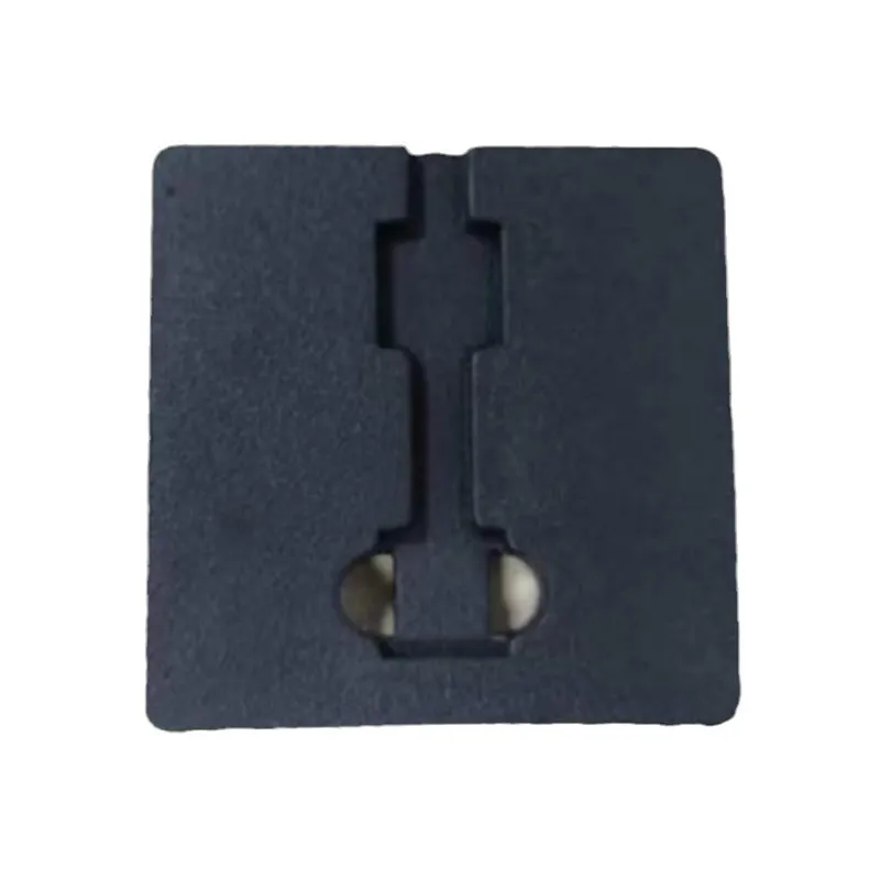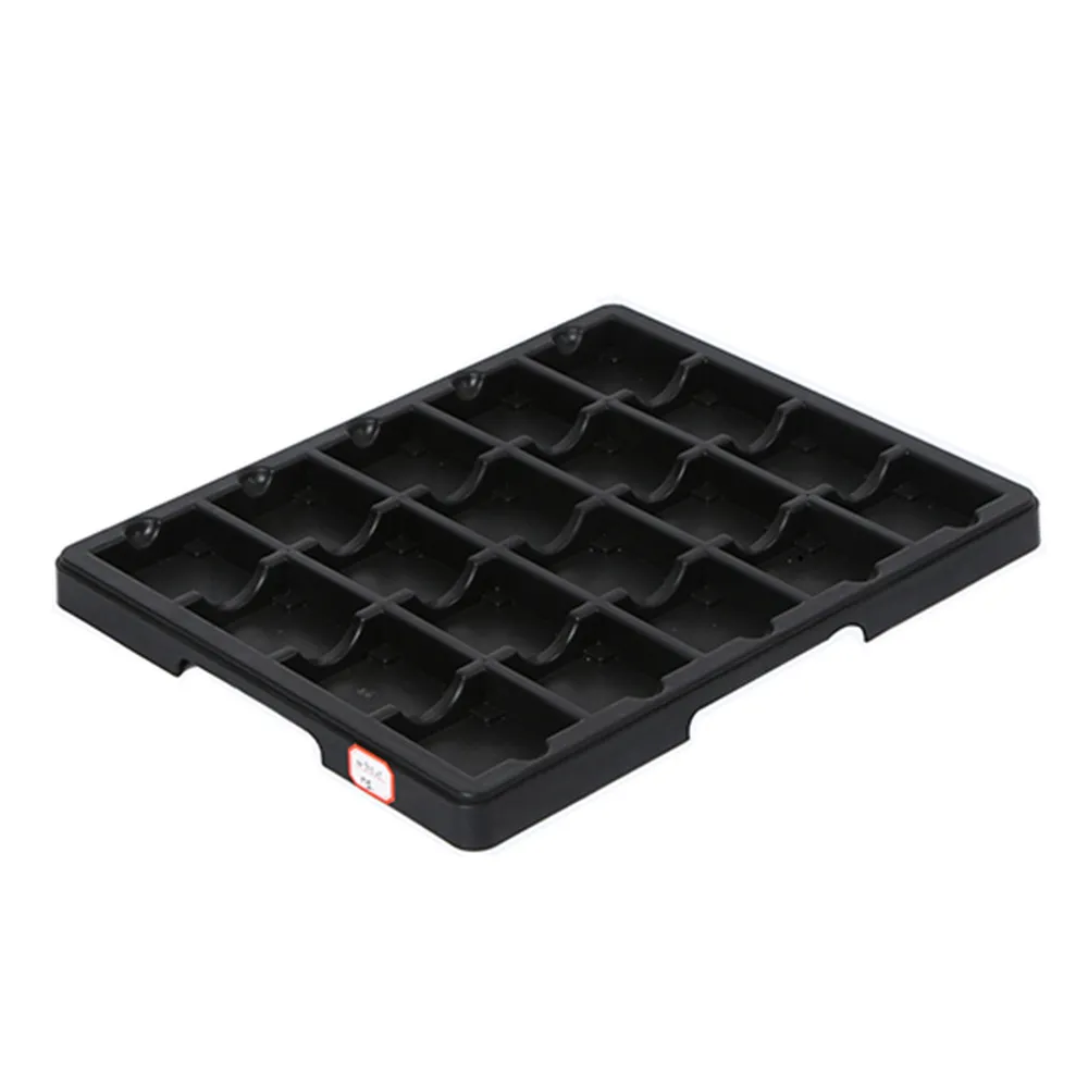
Лоток для микросхем, стандарт JEDEC, антистатический лоток для упаковки и тестирования чипов
Обзор
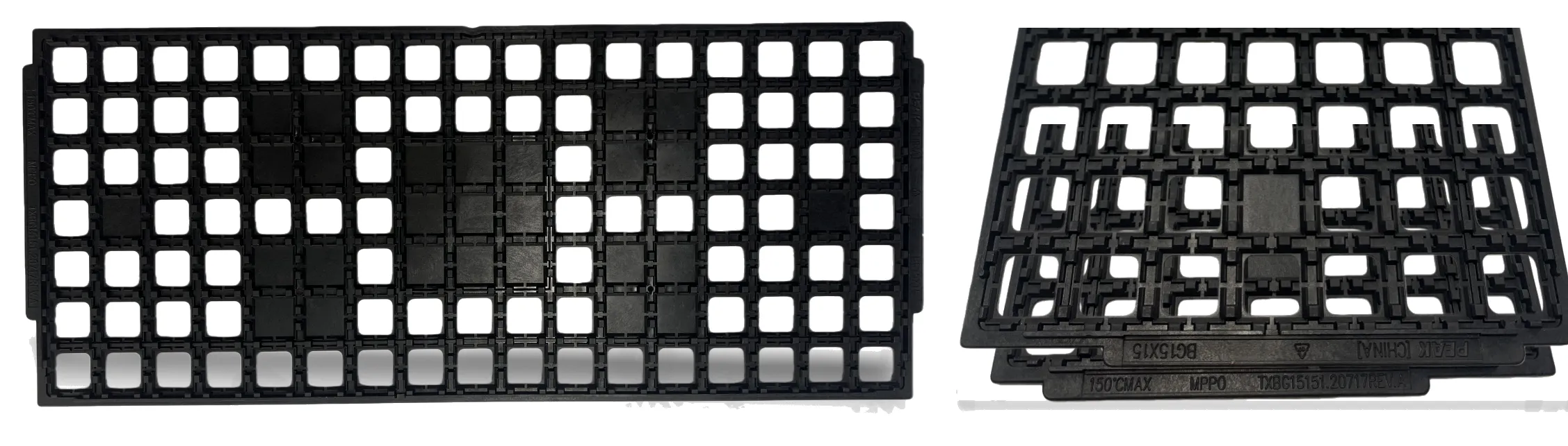
IC-лоток, также известный как лоток для электронных чипов, представляет собой пластиковый лоток, используемый компаниями по упаковке и тестированию полупроводников для упаковки и тестирования своих чипов (ИС), и соответствует международным стандартам JEDEC.
Введение продукта
IC tray, also known as electronic chip tray, is a plastic tray used by semiconductor packaging and testing companies for their chip (IC) packaging and testing, complies with JEDEC international standards.
Это может предотвратить электростатический контакт продукта, защитить чип от повреждений и облегчить автоматическое обнаружение и установку. Платформы для микросхем могут использоваться для различных методов упаковки, таких как BGA, QFN, QFP, PGA, TSOP, TQFP, LQFP, PLCC, SOC, SiP и т. д.
Требования к эксплуатационным характеристикам материала лотка для ИС
(1) Для обеспечения электростатической защиты чипа материал должен обладать антистатическими свойствами, и обычно его модифицируют путем добавления антистатических агентов, проводящей сажи или проводящих углеродных волокон.
(2) Перед сборкой микросхемы в терминале ее необходимо прокалить, чтобы избежать влаги внутри микросхемы, что требует термостойкости материала.
(3) Зазор между верхней и нижней поддонами должен удерживать выводы основного чипа, чтобы предотвратить их расшатывание, изгиб или поломку. Это требует определенной размерной стабильности материала. (4) Чтобы избежать воздействия влажной среды на чип, материал поддона должен обладать низким водопоглощением.
(5) Чтобы уменьшить загрязнение и снизить потери, материалы должны быть многоразовыми и подлежащими переработке.
Техническая спецификация
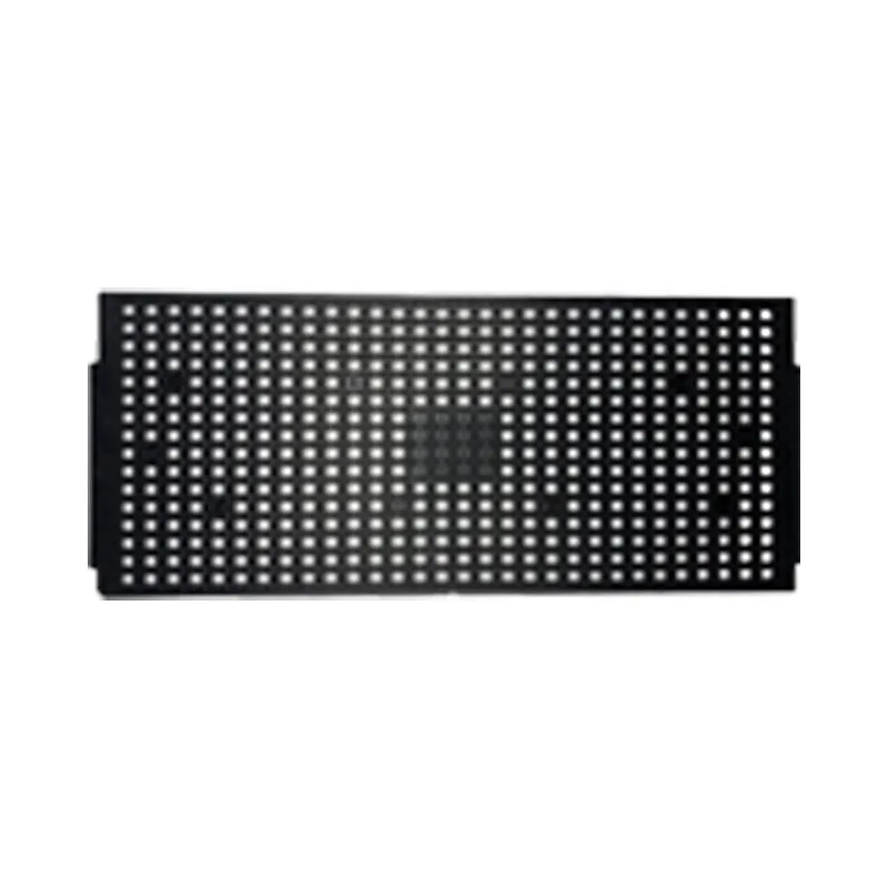
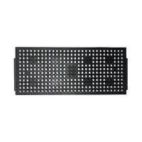
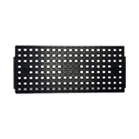
| Название товара | Лоток для микросхем | ||||
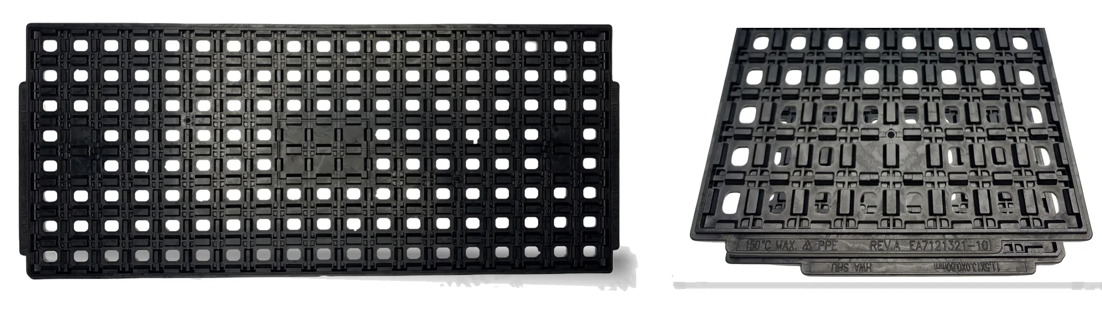
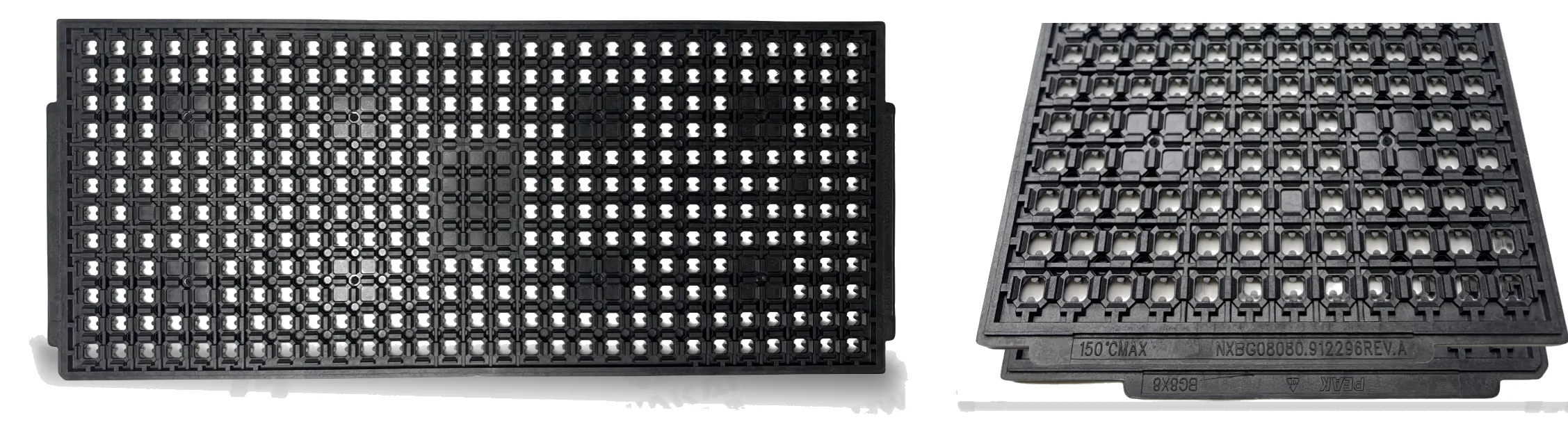
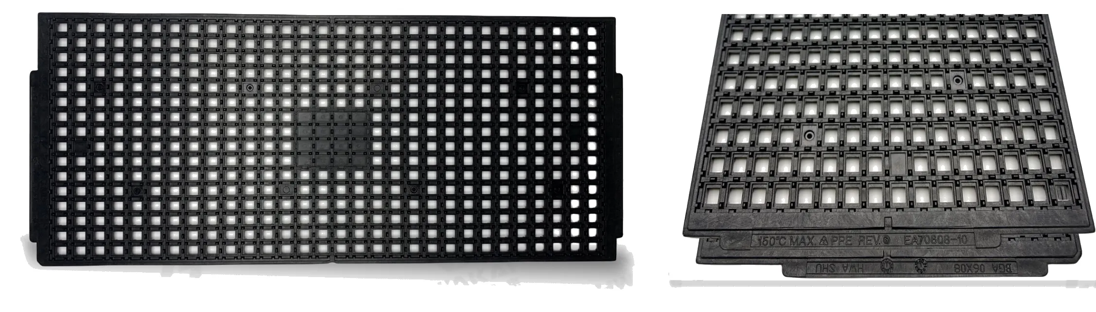
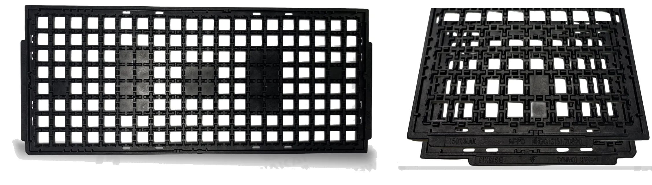
| Модель продукта | БГА6х8 | БГА8х8 | BGA11.5×13 | БГА13х13 | |
 |
 |
 |
 |
||
| Параметры спецификации | ●Модель | ЕА70608-10 | NXBG08080.912296REV.A | ЕА7121321-10 | НХБГ13131.70820 |
| ●Конструкция полости лотка | БГА | БГА | БГА | БГА | |
| ● Характеристики | 6*8 | 8*8 | 11.5*13*0.8 | 13*13 | |
| Матрица | 16*30=480 | 12*29=348 | 8*19=152 | 8*20=160 | |
| ●Максимальная температура (℃) | 150 | 150 | 150 | 150 | |
| ●Сопротивление поверхности | 10^5 (Ом) ~ 10^11 (Ом) | 10^5 (Ом) ~ 10^11 (Ом) | 10^5 (Ом) ~ 10^11 (Ом) | 10^5 (Ом) ~ 10^11 (Ом) | |
| ●Вес (г) | 138.5 | 162.4 | 125 | 110 | |
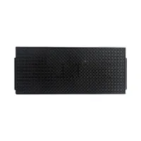
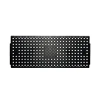
| Название товара | Лоток для микросхем | ||
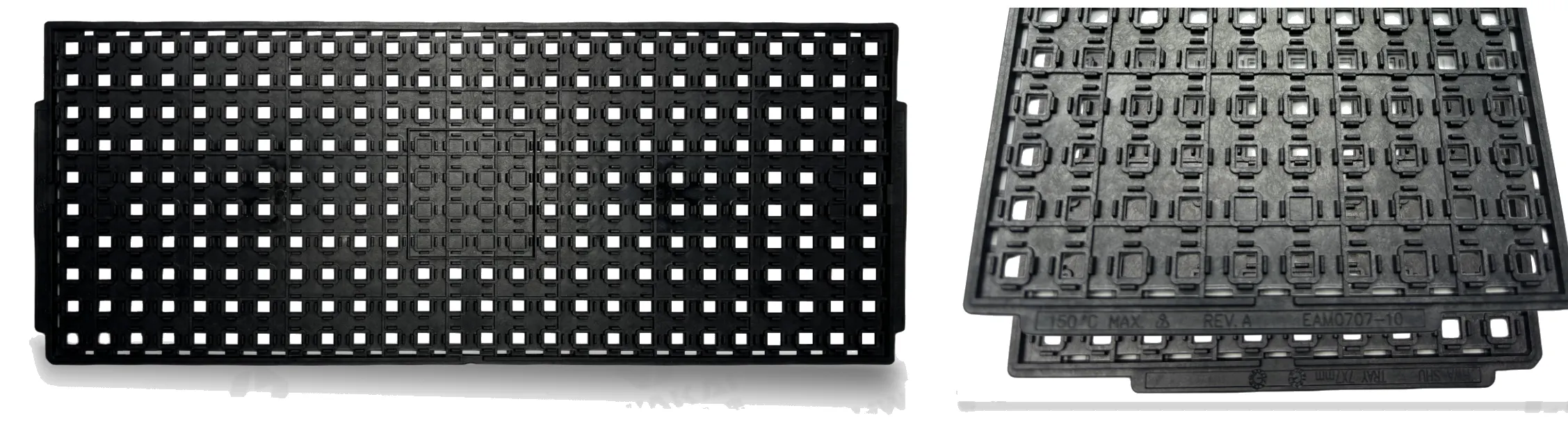
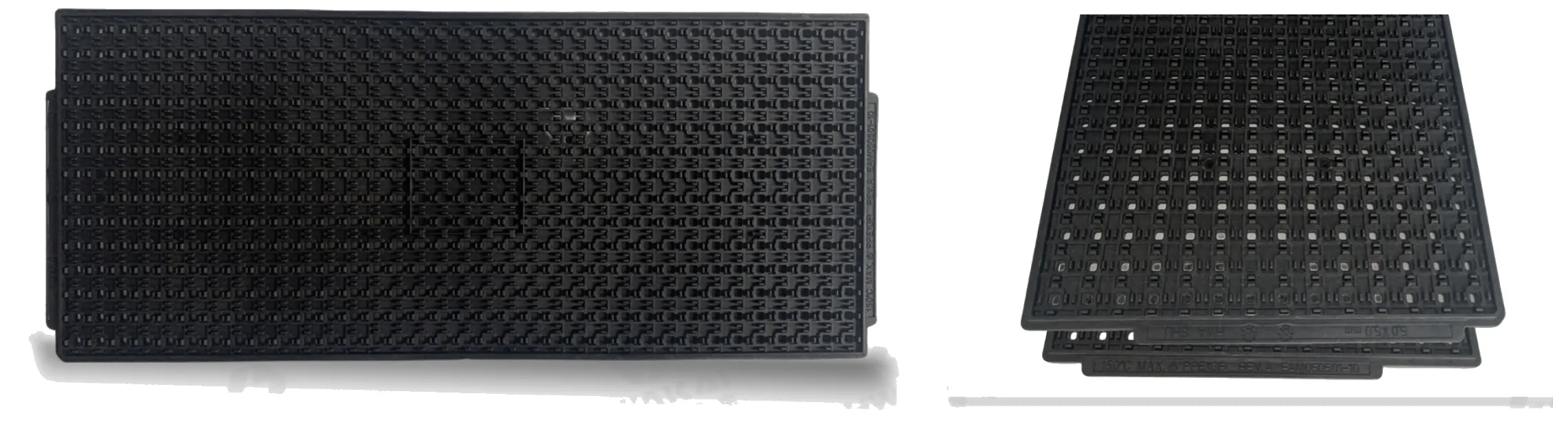
| Модель продукта | КФН5Х5 | QFN7x7 | |
 |
 |
||
| Параметры спецификации | ●Модель | ЕАМ050501-10 | EAM0707-10 |
| ●Конструкция полости лотка | КФН | КФН | |
| ● Характеристики | 5*5 | 7*7 | |
| Матрица | 14*35=490 | 10*26=260 | |
| ●Максимальная температура (℃) | 150 | 150 | |
| ●Сопротивление поверхности | 10^5 (Ом) ~ 10^11 (Ом) | 10^4(Ом)~10^11(Ом) | |
| ●Вес (г) | 183.9 | 148 | |
Производственные мощности мирового класса по защите от электростатических разрядов
При сотрудничестве с Sanwei вы напрямую взаимодействуете с ведущим в отрасли OEM/ODM-производителем. Мы управляем высокотехнологичным предприятием Интегрированный производственный комплекс площадью более 70 000 м² в Центральном индустриальном парке Юэцин провинции Чжэцзян, управляя каждым отдельным процессом от разработки собственной рецептуры материалов до окончательного формирования высокоточного изделия.
Интегрированная шкала
Передовой заводской комплекс площадью более 70 000 кв. м, оснащенный тяжелыми прецизионными литьевыми машинами для выполнения крупных оптовых заказов со стабильными сроками поставки.
Управление по всей цепочке
Полный производственный цикл собственными силами: от разработки собственных антистатических материалов и проектирования пресс-форм до автоматизированного производства и оперативной глобальной логистики.
Тщательная проверка
Строгий контроль сырья в сочетании с многоточечным измерением поверхностного удельного сопротивления на производственной линии гарантирует соответствие модели 100% требованиям международных стандартов по электростатической разрядке (ESD).
Антистатический Продукты и решения
Обеспечение комплексной электростатической защиты на всех этапах вашего производственного и операционного жизненного цикла.
SMT Оборудование
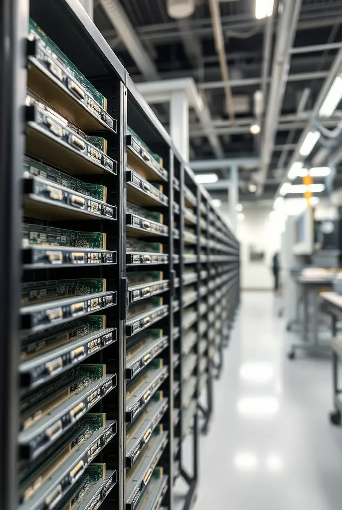
Антистатические накопительные ящики и стеллажи для автоматизированных линий.

Хранение и логистика
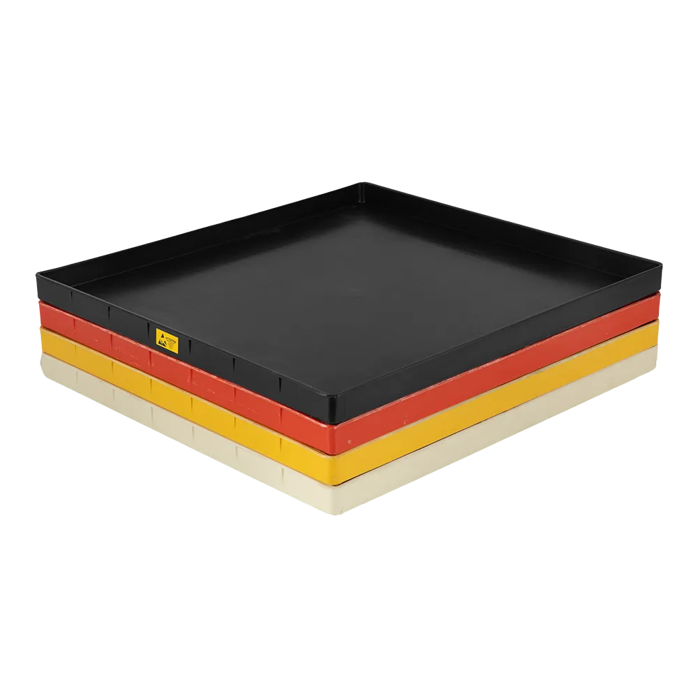
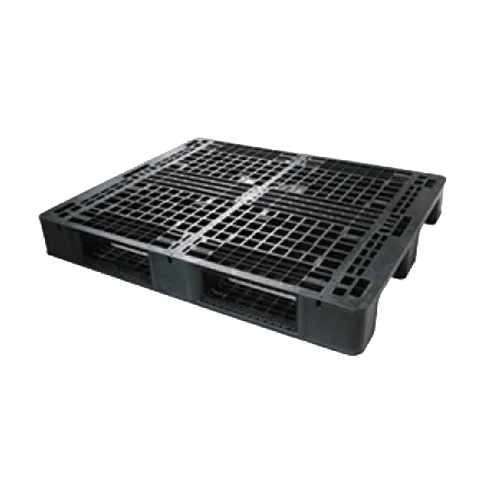
Тележки для оборота, стеллажи, коробки, лотки и контейнеры для комплектующих.

Рабочее место и СИЗ
Антистатические кресла, коврики, наручные ремни и средства индивидуальной защиты.
Заказная разработка
Разработка кастомных пресс-форм и специальные антистатические материалы.
Наши преимущества OEM/ODM

Передовые исследования и разработки и инновации в области материалов
Собственные антистатические материалы собственной разработки, защищенные национальными патентами на изобретения, с термостойкостью до 200℃. Мы не просто производим литье — мы создаем компаунды.

Производственная мощность в полном объеме
Завод площадью 30 000 кв. м с полным циклом систем литья под давлением, грануляции и вспомогательной обработки для обеспечения стабильных и эффективных поставок.

Полномасштабная кастомизация
Удельное электрическое сопротивление материалов, цвет, размер, логотип, упаковка и сертификаты могут быть адаптированы в соответствии с требованиями стандартов IEC61340-5-1, ANSI/ESD S20.20 или военных стандартов.

Сертифицированное качество и глобальное соответствие
“Компания Sanwei успешно разработала изготовленные по индивидуальному заказу термостойкие чистые поддоны натурального цвета для нашей линии сборки полупроводников, заменив импортную продукцию, обеспечив превосходную защиту от электростатических разрядов (ESD) и выполнив высокие требования чистоты цеха.”
НАМ ДОВЕРЯЮТ МИРОВЫЕ ЛИДЕРЫ ИНДУСТРИИ ИЗ СПИСКА FORTUNE 500
Наши запатентованные решения для защиты от электростатических разрядов используются на передовых производственных предприятиях по всему миру, включая: Intel, Motorola, Siemens, IBM, Panasonic, Nokia и Dell.
Ищете нестандартные размеры или оптовые цены?
Опираясь на нашу надежную собственную научно-исследовательскую группу, компания Sanwei предлагает полный спектр услуг OEM/ODM, адаптированных под ваши конкретные линии поверхностного монтажа (SMT) или планировку склада. Свяжитесь с нашими специалистами сегодня для заказа нестандартных пресс-форм, цветовой маркировки или комплексных консультаций по организации хранения по системе 5S.
Часто задаваемые вопросы (FAQ)
1. What is an IC tray?
It’s basically a plastic tray that holds semiconductor chips during manufacturing, testing, shipping, and storage. They’re specially made to be ESD‑safe so static doesn’t fry the chips. Most of them follow standard sizes so they work with automated handling equipment.
2. What are the materials used in IC packaging?
That’s a whole “package” of stuff – you’ve got the molding compound (usually epoxy resin), a substrate (organic or ceramic), lead frames, die attach adhesives, bonding wires, and solder balls. All these materials work together to protect the chip, connect it to the circuit, and help keep it cool.
3. What material are ice trays made of?
Ice trays for your freezer are a totally different story – they’re all about food safety. The most common are food‑grade polypropylene (PP) and silicone. Silicone’s nice because it’s flexible and makes popping out the ice cubes super easy.
4. What is the standard tray size?
When people say “standard tray,” they usually mean the JEDEC size – that’s 12.7 x 5.35 inches, or about 322.6 x 136 mm. Thickness can be either 0.25 inches (thin) or 0.40 inches (thick). There’s also a common 320mm x 240mm size used internationally.
5. What is a JEDEC tray?
It’s a tray that meets the specs set by JEDEC – the group that writes standards for the semiconductor industry. Think of it as a universal container for chips (like BGA or QFP packages) so that trays from different manufacturers all fit the same machines and processes.
6. What is the tolerance of JEDEC trays?
They’re made to pretty tight tolerances to make sure chips sit exactly right. For example, the dimension accuracy is often around ±0.15 mm, and the overall flatness is kept within about 0.76 mm. That said, the exact numbers can vary a bit between suppliers – always check the data sheet.
7. What is the JEDEC standard?
JEDEC is basically the rule‑maker for the microelectronics world. They publish standards for everything from memory chips (like DDR5) to how parts are packaged and tested. It’s the common language that makes sure chips from different companies can work together.
8. What is the difference between JEDEC and IPC?
Think of it this way: JEDEC focuses on the chip itself – its electrical specs, physical dimensions, and testing. IPC, on the other hand, deals with the circuit board and assembly – how PCBs are designed, manufactured, and soldered. So JEDEC is about the silicon, IPC is about the board.