IC Trays for Semiconductor and BGA Packaging
개요:
Review IC tray options for BGA and QFN devices. Request pocket drawings, material specifications, ESD evidence and samples for your handling process.
IC Trays for Semiconductor Handling and Packaging
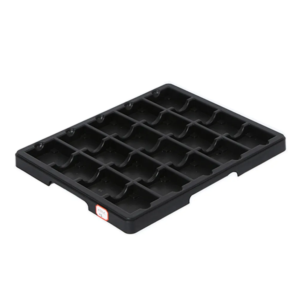
IC trays locate packaged semiconductor devices for controlled storage, inspection and handling. Select the pocket layout for the actual device package, permitted support areas and pickup process. SWESD’s catalogue on this page includes BGA and QFN tray options; confirm the current drawing and supplied configuration for the model you intend to purchase.
A tray’s appearance or an ESD description does not establish every required protective function. Ask for the relevant material and test evidence under your ESD control plan. Packaging used outside an ESD protected area may require discharge shielding as part of the complete package. See the EOS/ESD Association’s control principles for that distinction.
What to Confirm Before Ordering an IC Tray
- Device package drawing, pocket geometry, orientation and permitted contact surfaces.
- Tray outline, stacking interface and compatibility with the actual handling equipment.
- Material grade and the relevant electrical test method, conditions and results.
- Any required thermal exposure, its duration and the permitted supplier-defined conditions. Do not assume every device needs baking or every tray supports the same cycle.
- Sample acceptance, labeling, cleanliness, repeat supply and change notification requirements.
If JEDEC compatibility is required, specify the applicable current drawing or standard and request supporting evidence for the exact model. Confirming a tray outline does not by itself qualify the pocket, material or complete packaging arrangement for your device.
사용하세요 tray drawing review guide, pocket tolerance checklist 그리고 맞춤형 IC 트레이 견적 요청(RFQ) 가이드 to prepare a sample request. For the wider carrier range, browse SWESD ESD trays.
The catalogue figures below are product-listing information. Request the current supplier drawing, material specification, relevant test conditions and approved use limits before accepting a particular model for production. For a quotation, send your device drawing, handling route, quantity and evidence requirements through the SWESD inquiry page.
기술 사양서
Scroll the specification tables horizontally to compare all listed models.
| 제품명 | IC 트레이 | ||||
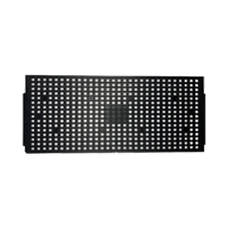
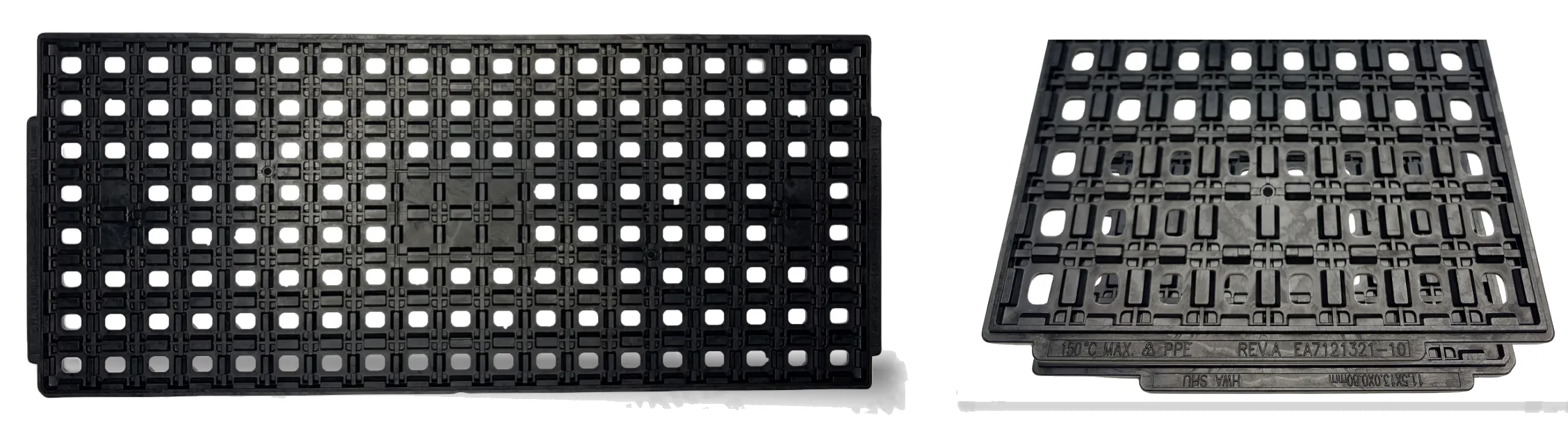
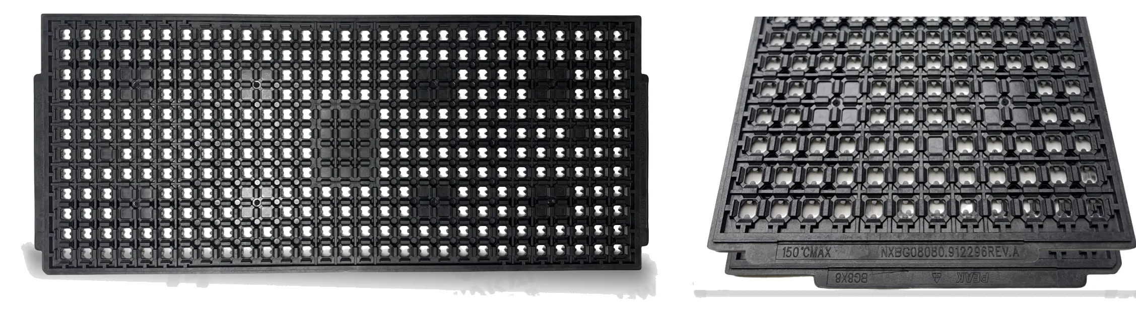
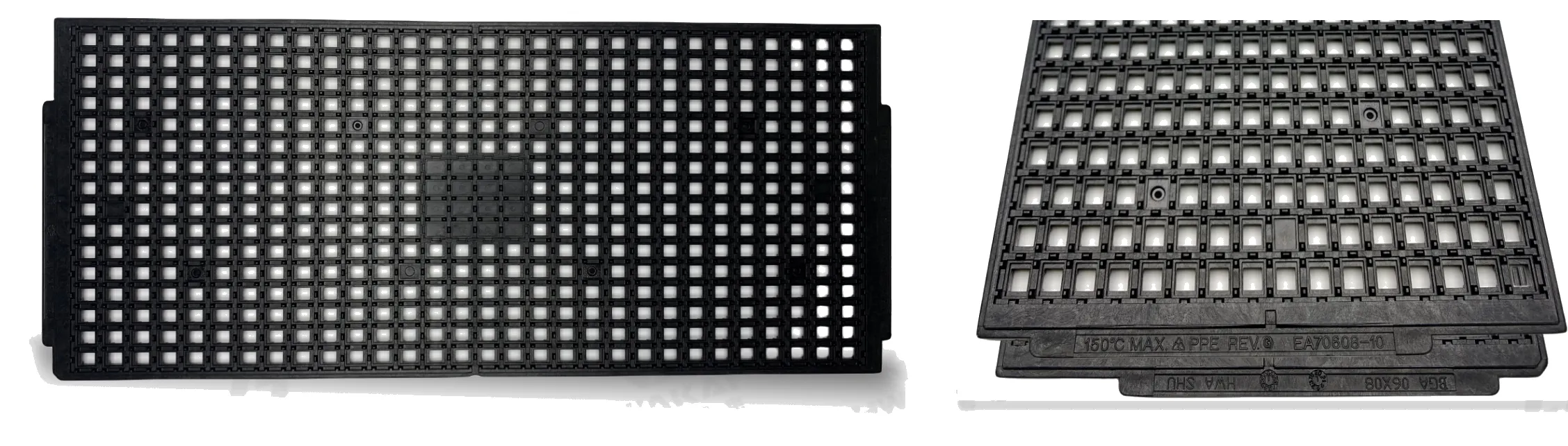
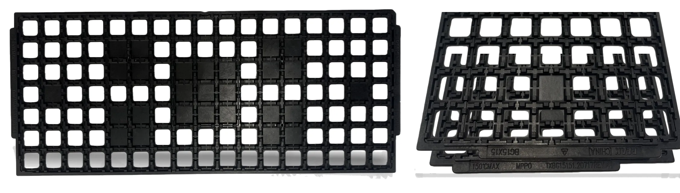
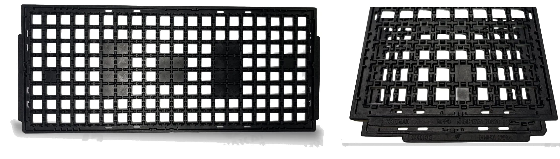
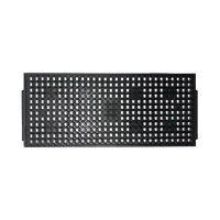
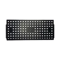
| 제품 모델 | BGA6x8 | BGA8x8 | BGA11.5×13 | BGA13x13 | |
 |
 |
 |
 |
||
| 사양 매개변수 | ●Model | EA70608-10 | NXBG08080.912296REV.A | EA7121321-10 | NHBG13131.70820 |
| ●Tray cavity design | BGA | BGA | BGA | BGA | |
| ●Specifications | 6*8 | 8*8 | 11.5*13*0.8 | 13*13 | |
| ●Matrix | 16*30=480 | 12*29=348 | 8*19=152 | 8*20=160 | |
| ●Temperature MAX (℃) | 150 | 150 | 150 | 150 | |
| ●Surface Resistance | 10^5(Ω)~10^11(Ω) | 10^5(Ω)~10^11(Ω) | 10^5(Ω)~10^11(Ω) | 10^5(Ω)~10^11(Ω) | |
| ●Weight (g) | 138.5 | 162.4 | 125 | 110 | |
| 제품명 | IC 트레이 | ||
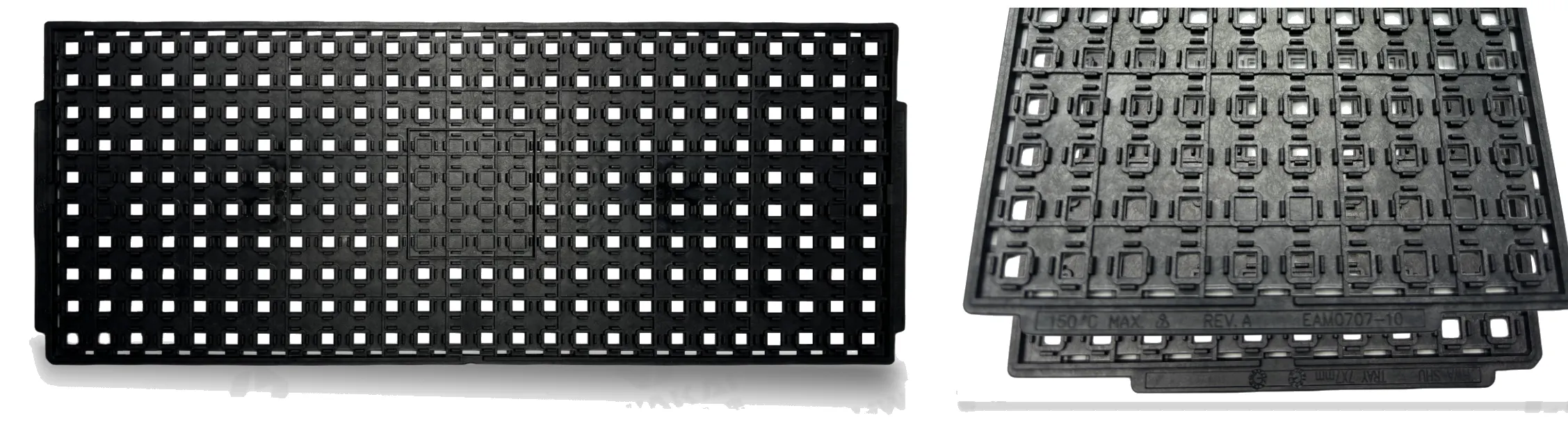
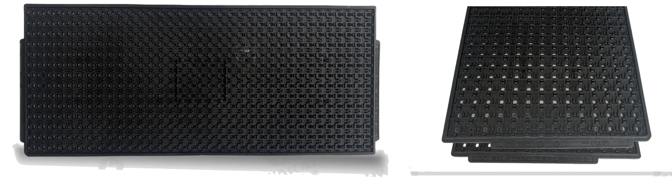
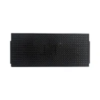
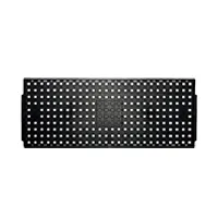
| 제품 모델 | QFN5x5 | QFN7x7 | |
 |
 |
||
| 사양 매개변수 | ●Model | EAM050501-10 | EAM0707-10 |
| ●Tray cavity design | QFN | QFN | |
| ●Specifications | 5*5 | 7*7 | |
| ●Matrix | 14*35=490 | 10*26=260 | |
| ●Temperature MAX (℃) | 150 | 150 | |
| ●Surface Resistance | 10^5(Ω)~10^11(Ω) | 10^4(Ω)~10^11(Ω) | |
| ●Weight (g) | 183.9 | 148 | |
세계 최고 수준의 ESD 제조 역량
삼웨이(Sanwei)에서 소싱하시면, 업계 선두의 OEM/ODM 제조업체와 직접 파트너십을 맺게 되는 것입니다. 당사는 최첨단 70,000제곱미터 이상 규모의 통합 생산 시설 저장성 웨칭 중앙 산업단지에서 독자적인 소재 배합부터 최종 고정밀 제품 성형에 이르기까지 모든 공정을 관리합니다.
통합 저울
7만 제곱미터 이상의 첨단 공장 기지에 대형 정밀 사출기를 갖추어, 안정적인 납기로 대량 도매 주문을 처리합니다.
전 과정 제어
독자적인 정전기 방지 소재 연구개발, 구조용 금형 엔지니어링, 자동화 제조, 그리고 신속한 글로벌 물류 배송에 이르는 완벽한 자체 통합 제어.
엄격한 검사
엄격한 원자재 검사 및 생산 라인에서의 다점 표면 저항률 측정을 통해 100% 제품이 국제 ESD 표준 지침을 준수함을 보장합니다.
정전기 방지 제품 및 솔루션
제조 및 운영 수명 주기 전반에 걸쳐 포괄적인 정전기 보호를 제공합니다.
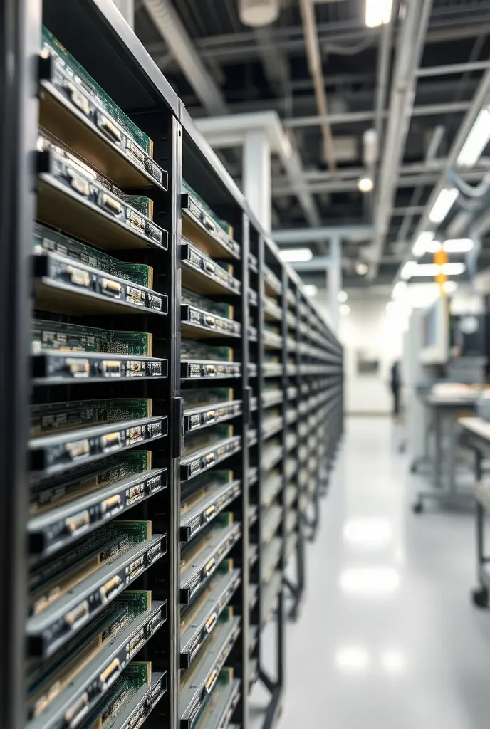
SMT 장비
자동화 라인용 제전 수납함 및 랙.

보관 및 물류
대차, 선반, 상자, 트레이 및 부품 용기.

작업대 및 개인 보호 장구
정전기 방지 의자, 매트, 손목 스트랩 및 개인 보호구.
맞춤형 개발
맞춤형 금형 개발 및 특수 제전 소재.
당사의 OEM/ODM 장점

첨단 R&D 및 소재 혁신
국가 발명 특허를 보유하고 최대 200℃의 내열성을 갖춘 자체 개발 대전방지 소재. 당사는 단순 성형에 그치지 않고 컴파운드를 직접 배합합니다.

양산 능력
안정적이고 효율적인 공급을 위해 완전 사출 성형, 조립 및 부대 가공 시스템을 갖춘 30,000㎡ 규모의 공장.

전 과정 맞춤 제작
재질 저항률, 색상, 크기, 로고, 포장 및 인증 — IEC61340-5-1, ANSI/ESD S20.20 또는 군사 규격에 맞게 맞춤 제작 가능합니다.

공인된 품질 및 글로벌 컴플라이언스
“산웨이는 반도체 조립 라인을 위한 맞춤형 고내열성 클린 내추럴 컬러 트레이를 성공적으로 개발하여 수입 제품을 대체하고, 우수한 ESD 안전성을 확보하며, 작업장의 높은 청정도 요구 사항을 충족했습니다.”
글로벌 포춘 500대 업계 리더들이 신뢰하는 기업
당사의 독자적인 ESD 솔루션은 다음을 포함하여 전 세계의 우수 생산 시설에 구축되어 있습니다. 인텔, 모토로라, 지멘스, IBM, 파나소닉, 노키아, 델.
맞춤 제작 사이즈나 대량 도매 가격을 찾고 계신가요?
당사의 강력한 자체 R&D 팀을 바탕으로, 싼웨이는 귀사의 특정 SMT 생산 라인 또는 창고 레이아웃에 맞춤화된 완전한 OEM/ODM 옵션을 제공합니다. 맞춤형 금형, 색상 코딩 또는 통합 5S 보관 컨설팅을 위해 지금 당사 전문가에게 문의하십시오.
자주 묻는 질문 (FAQ)
1. What is an IC tray?
It’s basically a plastic tray that holds semiconductor chips during manufacturing, testing, shipping, and storage. They’re specially made to be ESD‑safe so static doesn’t fry the chips. Most of them follow standard sizes so they work with automated handling equipment.
2. What are the materials used in IC packaging?
That’s a whole “package” of stuff – you’ve got the molding compound (usually epoxy resin), a substrate (organic or ceramic), lead frames, die attach adhesives, bonding wires, and solder balls. All these materials work together to protect the chip, connect it to the circuit, and help keep it cool.
3. What material are ice trays made of?
Ice trays for your freezer are a totally different story – they’re all about food safety. The most common are food‑grade polypropylene (PP) and silicone. Silicone’s nice because it’s flexible and makes popping out the ice cubes super easy.
4. What is the standard tray size?
When people say “standard tray,” they usually mean the JEDEC size – that’s 12.7 x 5.35 inches, or about 322.6 x 136 mm. Thickness can be either 0.25 inches (thin) or 0.40 inches (thick). There’s also a common 320mm x 240mm size used internationally.
5. What is a JEDEC tray?
It’s a tray that meets the specs set by JEDEC – the group that writes standards for the semiconductor industry. Think of it as a universal container for chips (like BGA or QFP packages) so that trays from different manufacturers all fit the same machines and processes.
6. What is the tolerance of JEDEC trays?
They’re made to pretty tight tolerances to make sure chips sit exactly right. For example, the dimension accuracy is often around ±0.15 mm, and the overall flatness is kept within about 0.76 mm. That said, the exact numbers can vary a bit between suppliers – always check the data sheet.
7. What is the JEDEC standard?
JEDEC is basically the rule‑maker for the microelectronics world. They publish standards for everything from memory chips (like DDR5) to how parts are packaged and tested. It’s the common language that makes sure chips from different companies can work together.
8. What is the difference between JEDEC and IPC?
Think of it this way: JEDEC focuses on the chip itself – its electrical specs, physical dimensions, and testing. IPC, on the other hand, deals with the circuit board and assembly – how PCBs are designed, manufactured, and soldered. So JEDEC is about the silicon, IPC is about the board.