IC Trays for Semiconductor and BGA Packaging
Resumen:
Review IC tray options for BGA and QFN devices. Request pocket drawings, material specifications, ESD evidence and samples for your handling process.
IC Trays for Semiconductor Handling and Packaging
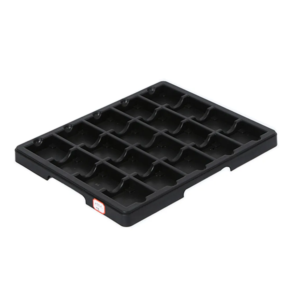
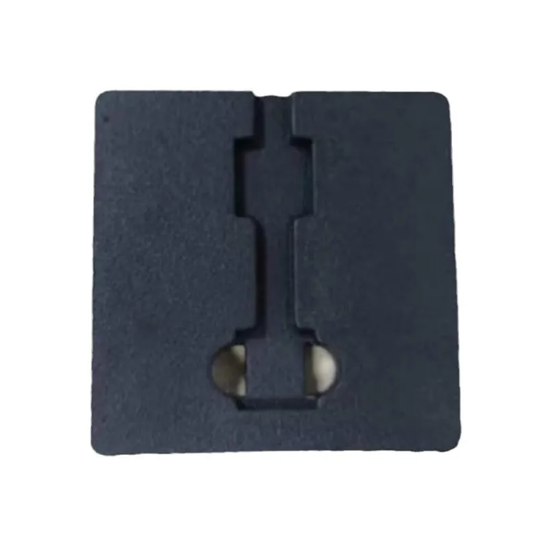
IC trays locate packaged semiconductor devices for controlled storage, inspection and handling. Select the pocket layout for the actual device package, permitted support areas and pickup process. SWESD’s catalogue on this page includes BGA and QFN tray options; confirm the current drawing and supplied configuration for the model you intend to purchase.
A tray’s appearance or an ESD description does not establish every required protective function. Ask for the relevant material and test evidence under your ESD control plan. Packaging used outside an ESD protected area may require discharge shielding as part of the complete package. See the EOS/ESD Association’s control principles for that distinction.
What to Confirm Before Ordering an IC Tray
- Device package drawing, pocket geometry, orientation and permitted contact surfaces.
- Tray outline, stacking interface and compatibility with the actual handling equipment.
- Material grade and the relevant electrical test method, conditions and results.
- Any required thermal exposure, its duration and the permitted supplier-defined conditions. Do not assume every device needs baking or every tray supports the same cycle.
- Sample acceptance, labeling, cleanliness, repeat supply and change notification requirements.
If JEDEC compatibility is required, specify the applicable current drawing or standard and request supporting evidence for the exact model. Confirming a tray outline does not by itself qualify the pocket, material or complete packaging arrangement for your device.
Utiliza el tray drawing review guide, pocket tolerance checklist y Guía de Solicitud de Cotización (RFQ) para bandejas de circuitos integrados (IC) personalizadas to prepare a sample request. For the wider carrier range, browse SWESD ESD trays.
The catalogue figures below are product-listing information. Request the current supplier drawing, material specification, relevant test conditions and approved use limits before accepting a particular model for production. For a quotation, send your device drawing, handling route, quantity and evidence requirements through the SWESD inquiry page.
Technical Specification
Scroll the specification tables horizontally to compare all listed models.
| Product name | bandeja de circuitos integrados | ||||
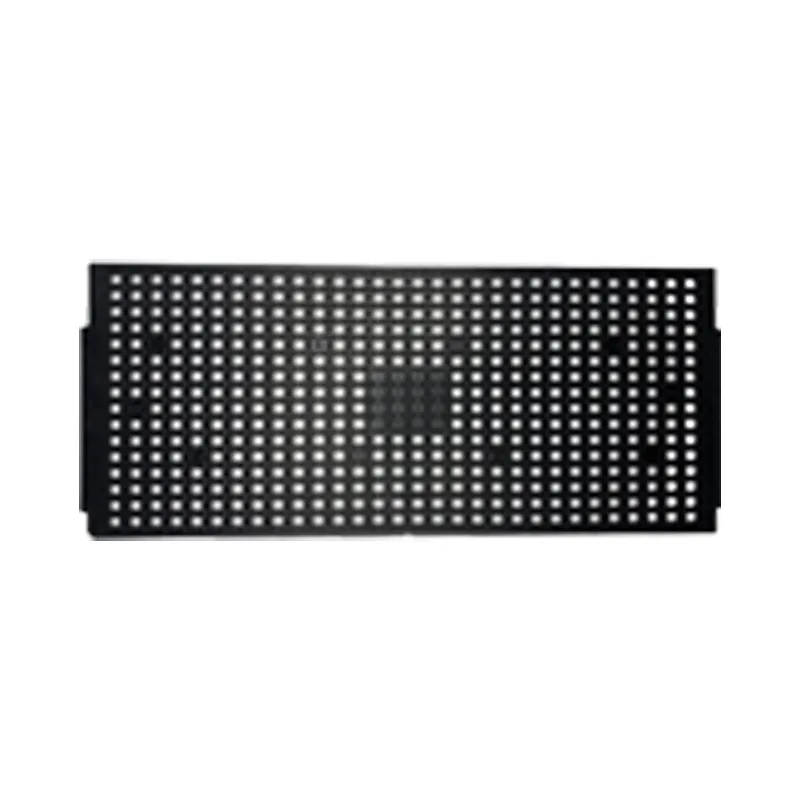
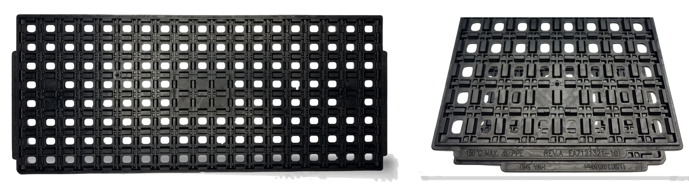
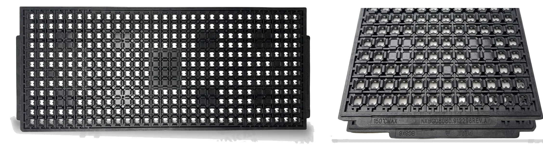
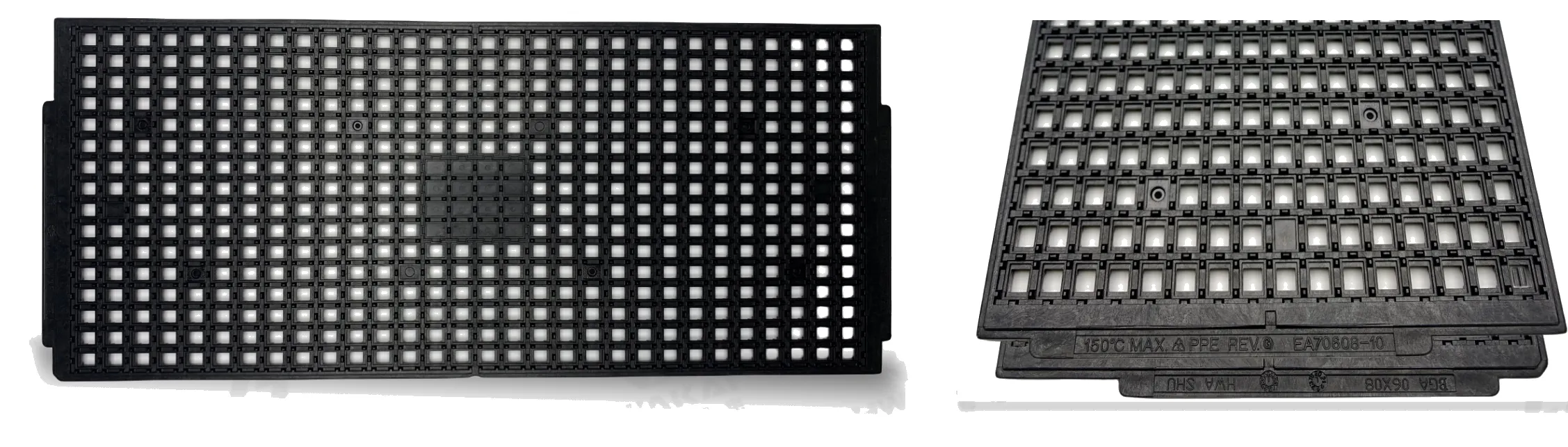
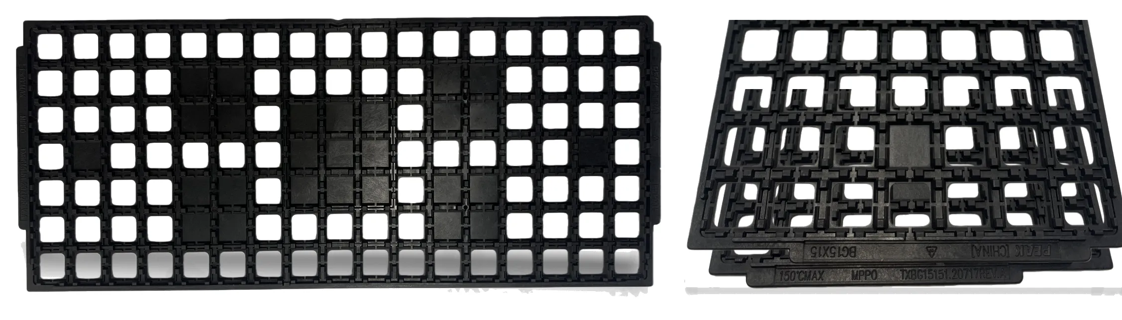
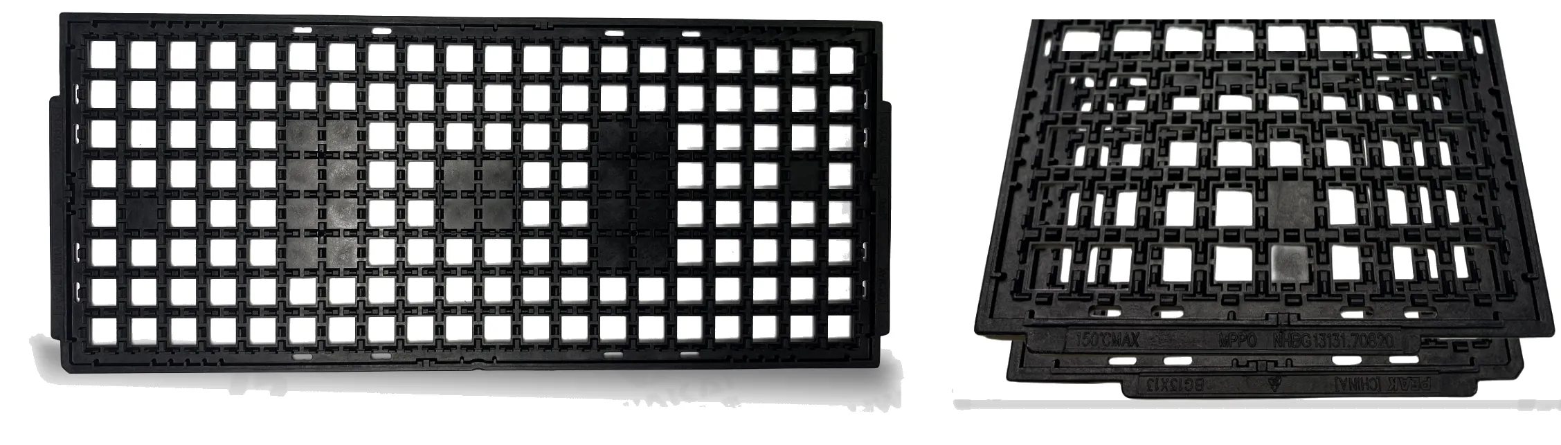
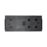
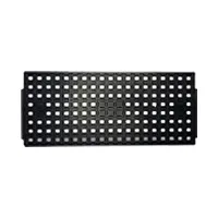
| Product model | BGA6x8 | BGA8x8 | BGA11.5×13 | BGA13x13 | |
 |
 |
 |
 |
||
| Specification parameters | ●Model | EA70608-10 | NXBG08080.912296REV.A | EA7121321-10 | NHBG13131.70820 |
| ●Tray cavity design | BGA | BGA | BGA | BGA | |
| ●Specifications | 6*8 | 8*8 | 11.5*13*0.8 | 13*13 | |
| ●Matrix | 16*30=480 | 12*29=348 | 8*19=152 | 8*20=160 | |
| ●Temperature MAX (℃) | 150 | 150 | 150 | 150 | |
| ●Surface Resistance | 10^5(Ω)~10^11(Ω) | 10^5(Ω)~10^11(Ω) | 10^5(Ω)~10^11(Ω) | 10^5(Ω)~10^11(Ω) | |
| ●Weight (g) | 138.5 | 162.4 | 125 | 110 | |
| Product name | bandeja de circuitos integrados | ||
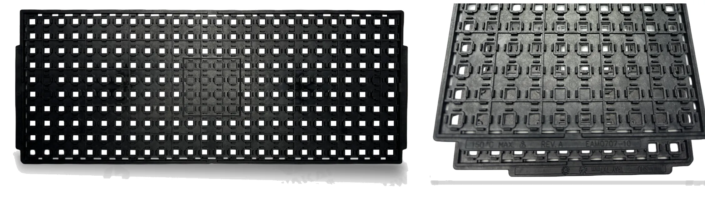
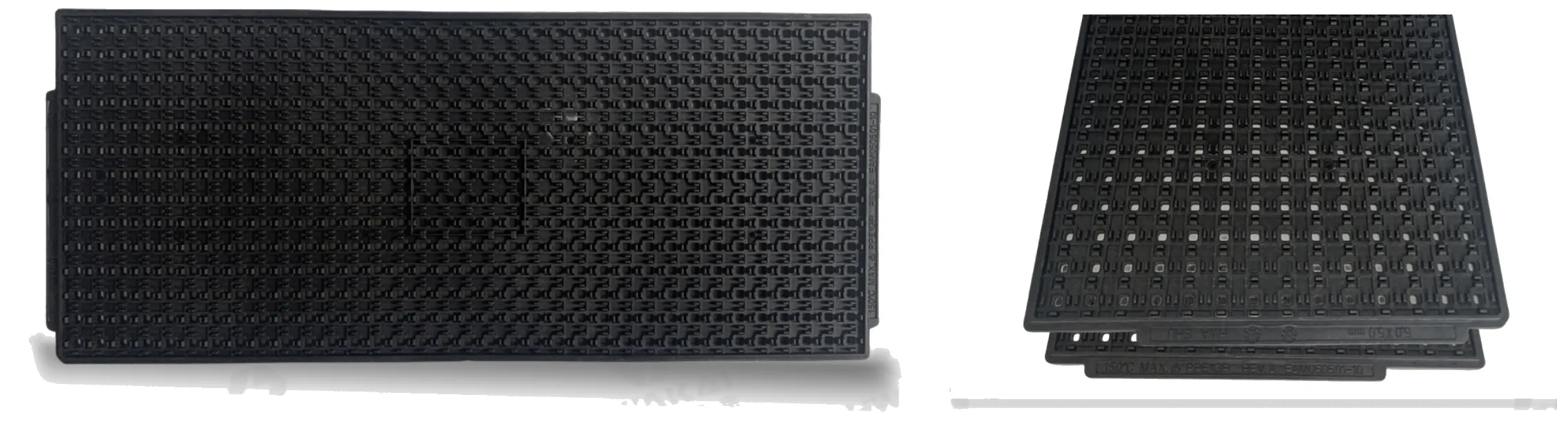
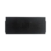
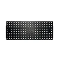
| Product model | QFN5x5 | QFN7x7 | |
 |
 |
||
| Specification parameters | ●Model | EAM050501-10 | EAM0707-10 |
| ●Tray cavity design | QFN | QFN | |
| ●Specifications | 5*5 | 7*7 | |
| ●Matrix | 14*35=490 | 10*26=260 | |
| ●Temperature MAX (℃) | 150 | 150 | |
| ●Surface Resistance | 10^5(Ω)~10^11(Ω) | 10^4(Ω)~10^11(Ω) | |
| ●Weight (g) | 183.9 | 148 | |
Capacidad de fabricación ESD de clase mundial
Al abastecerse de Sanwei, se está asociando directamente con un fabricante OEM/ODM líder en la industria. Operamos unas instalaciones de vanguardia Instalación de producción integrada de más de 70 000 m² en el Parque Industrial Central de Yueqing, Zhejiang, gestionando cada proceso, desde la formulación de materiales patentados hasta el moldeado final de productos de alta precisión.
Balanza integrada
Base de producción avanzada de más de 70.000 m² equipada con máquinas de moldeo por inyección de precisión para trabajos pesados para gestionar pedidos al por mayor con plazos de entrega estables.
Control de cadena completa
Control interno completo que abarca la investigación y desarrollo de material antiestático propio, ingeniería de moldes estructurales, fabricación automatizada y entrega rápida de logística global.
Inspección rigurosa
Los rigurosos ensayos de las materias primas, combinados con mediciones multipunto de la resistividad superficial en la línea de producción, garantizan que el 100% cumpla con las directrices de las normas internacionales sobre ESD.
Antiestático Productos y Soluciones
Ofreciendo protección electrostática integral en todo su ciclo de vida operativo y de fabricación.
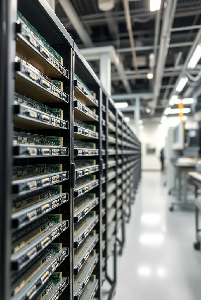
Equipos SMT
Cajas y soportes antiestáticos para líneas automatizadas.

Almacenamiento y Logística
Carros de rotación, estantes, cajas, bandejas y contenedores de componentes.

Estación de trabajo y EPP
Sillas antiestáticas, alfombrillas, pulseras antiestáticas y protección personal.
Desarrollo a medida
Desarrollo de moldes personalizados y materiales antiestáticos especiales.
NUESTRAS VENTAJAS OEM/ODM

I+D Avanzada e Innovación de Materiales
Materiales antiestáticos desarrollados internamente con patentes de invención nacionales y resistencia al calor de hasta 200 ℃. Nosotros no solo moldeamos, formulamos compuestos.

Capacidad de producción a escala completa
Planta de 30.000 m² con sistemas completos de moldeo por inyección, granulación y procesamiento auxiliar para un suministro estable y eficiente.

Personalización de proceso completo
Resistividad del material, color, tamaño, logotipo, embalaje y certificaciones — personalizables para cumplir con las normas IEC61340-5-1, ANSI/ESD S20.20 o estándares militares.

Calidad Certificada y Cumplimiento Global
“Sanwei desarrolló con éxito bandejas personalizadas de color natural limpio y resistentes a altas temperaturas para nuestra línea de ensamblaje de semiconductores, reemplazando productos importados, garantizando una excelente seguridad ESD y cumpliendo con los altos requisitos de limpieza del taller.”
CON LA CONFIANZA DE LOS LÍDERES INDUSTRIALES GLOBALES DE FORTUNE 500
Nuestras soluciones ESD patentadas se implementan en instalaciones de producción de élite en todo el mundo, incluidas: Intel, Motorola, Siemens, IBM, Panasonic, Nokia y Dell.
¿Busca tamaños personalizados o precios de venta al por mayor?
Respaldado por nuestro sólido equipo interno de I+D, Sanwei ofrece opciones completas de OEM/ODM adaptadas a sus líneas de producción SMT específicas o a la disposición de su almacén. Póngase en contacto con nuestros especialistas hoy mismo para obtener moldes personalizados, códigos de colores o asesoramiento integrado de almacenamiento 5S.
Preguntas frecuentes (FAQ)
1. What is an IC tray?
It’s basically a plastic tray that holds semiconductor chips during manufacturing, testing, shipping, and storage. They’re specially made to be ESD‑safe so static doesn’t fry the chips. Most of them follow standard sizes so they work with automated handling equipment.
2. What are the materials used in IC packaging?
That’s a whole “package” of stuff – you’ve got the molding compound (usually epoxy resin), a substrate (organic or ceramic), lead frames, die attach adhesives, bonding wires, and solder balls. All these materials work together to protect the chip, connect it to the circuit, and help keep it cool.
3. What material are ice trays made of?
Ice trays for your freezer are a totally different story – they’re all about food safety. The most common are food‑grade polypropylene (PP) and silicone. Silicone’s nice because it’s flexible and makes popping out the ice cubes super easy.
4. What is the standard tray size?
When people say “standard tray,” they usually mean the JEDEC size – that’s 12.7 x 5.35 inches, or about 322.6 x 136 mm. Thickness can be either 0.25 inches (thin) or 0.40 inches (thick). There’s also a common 320mm x 240mm size used internationally.
5. What is a JEDEC tray?
It’s a tray that meets the specs set by JEDEC – the group that writes standards for the semiconductor industry. Think of it as a universal container for chips (like BGA or QFP packages) so that trays from different manufacturers all fit the same machines and processes.
6. What is the tolerance of JEDEC trays?
They’re made to pretty tight tolerances to make sure chips sit exactly right. For example, the dimension accuracy is often around ±0.15 mm, and the overall flatness is kept within about 0.76 mm. That said, the exact numbers can vary a bit between suppliers – always check the data sheet.
7. What is the JEDEC standard?
JEDEC is basically the rule‑maker for the microelectronics world. They publish standards for everything from memory chips (like DDR5) to how parts are packaged and tested. It’s the common language that makes sure chips from different companies can work together.
8. What is the difference between JEDEC and IPC?
Think of it this way: JEDEC focuses on the chip itself – its electrical specs, physical dimensions, and testing. IPC, on the other hand, deals with the circuit board and assembly – how PCBs are designed, manufactured, and soldered. So JEDEC is about the silicon, IPC is about the board.