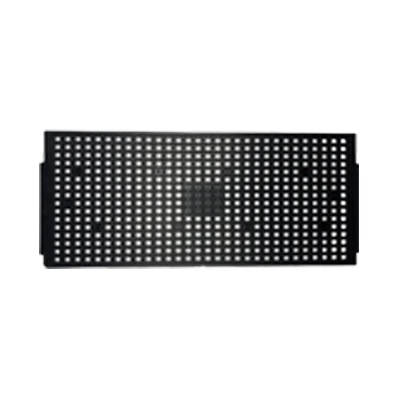
IC Trays for Semiconductor and BGA Packaging
Overzicht:
Review IC tray options for BGA and QFN devices. Request pocket drawings, material specifications, ESD evidence and samples for your handling process.
IC Trays for Semiconductor Handling and Packaging
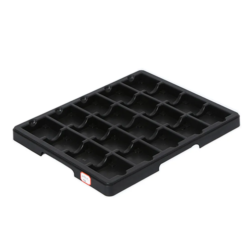
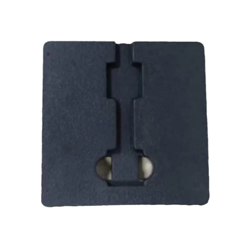
IC trays locate packaged semiconductor devices for controlled storage, inspection and handling. Select the pocket layout for the actual device package, permitted support areas and pickup process. SWESD’s catalogue on this page includes BGA and QFN tray options; confirm the current drawing and supplied configuration for the model you intend to purchase.
A tray’s appearance or an ESD description does not establish every required protective function. Ask for the relevant material and test evidence under your ESD control plan. Packaging used outside an ESD protected area may require discharge shielding as part of the complete package. See the EOS/ESD Association’s control principles for that distinction.
What to Confirm Before Ordering an IC Tray
- Device package drawing, pocket geometry, orientation and permitted contact surfaces.
- Tray outline, stacking interface and compatibility with the actual handling equipment.
- Material grade and the relevant electrical test method, conditions and results.
- Any required thermal exposure, its duration and the permitted supplier-defined conditions. Do not assume every device needs baking or every tray supports the same cycle.
- Sample acceptance, labeling, cleanliness, repeat supply and change notification requirements.
If JEDEC compatibility is required, specify the applicable current drawing or standard and request supporting evidence for the exact model. Confirming a tray outline does not by itself qualify the pocket, material or complete packaging arrangement for your device.
Gebruik de tray drawing review guide, pocket tolerance checklist en handleiding voor RFQ van aangepaste IC-trays to prepare a sample request. For the wider carrier range, browse SWESD ESD trays.
The catalogue figures below are product-listing information. Request the current supplier drawing, material specification, relevant test conditions and approved use limits before accepting a particular model for production. For a quotation, send your device drawing, handling route, quantity and evidence requirements through the SWESD inquiry page.
Technische specificatie
Scroll the specification tables horizontally to compare all listed models.
| Productnaam | IC-tray | ||||
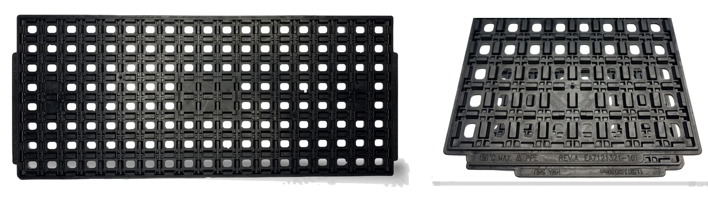
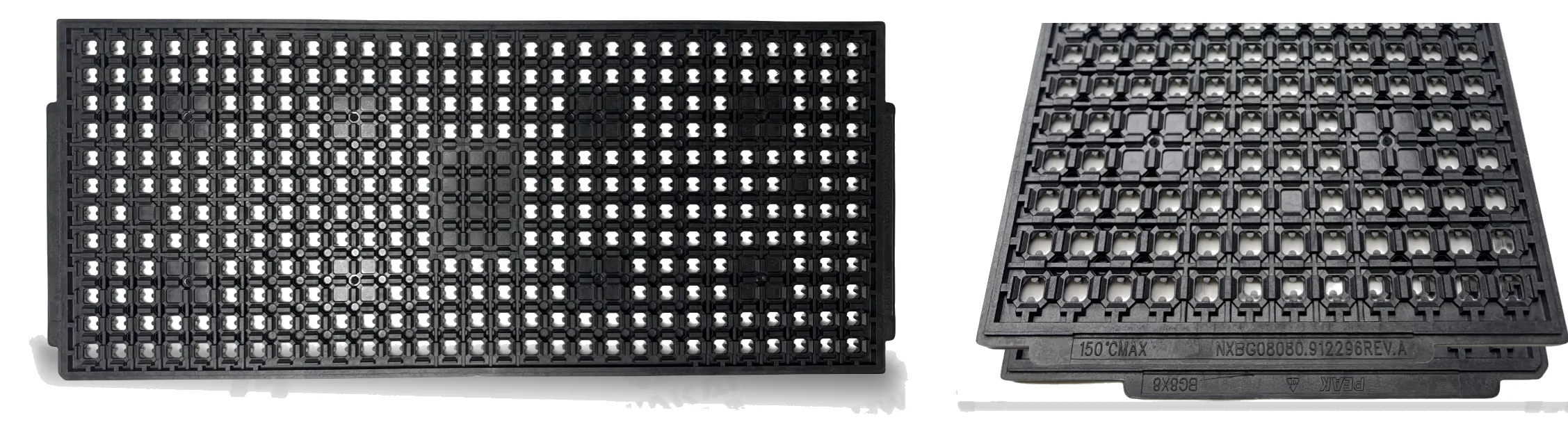
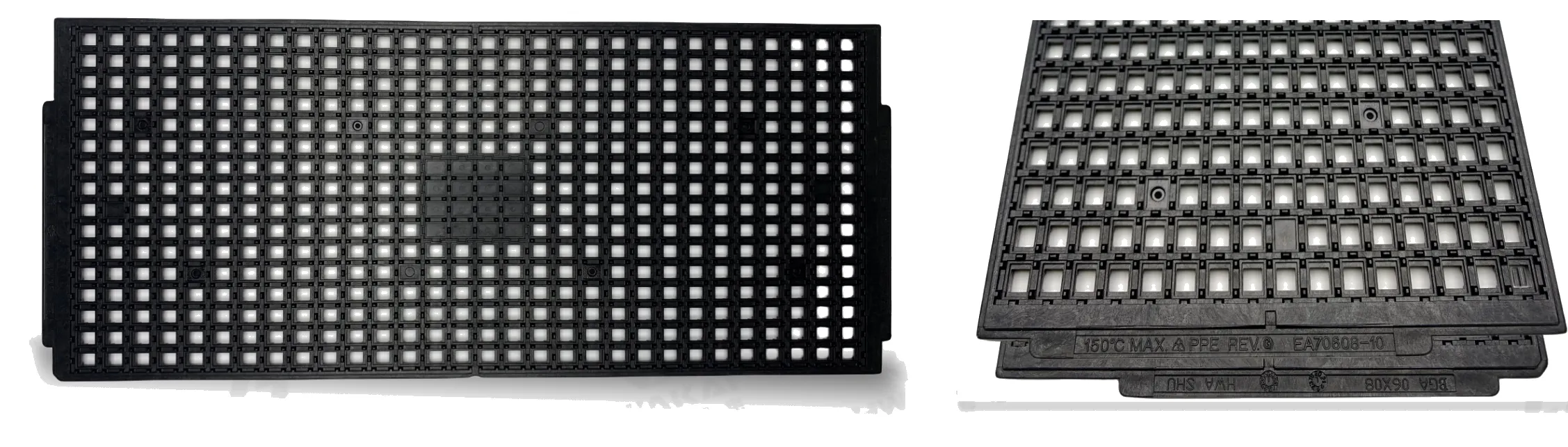
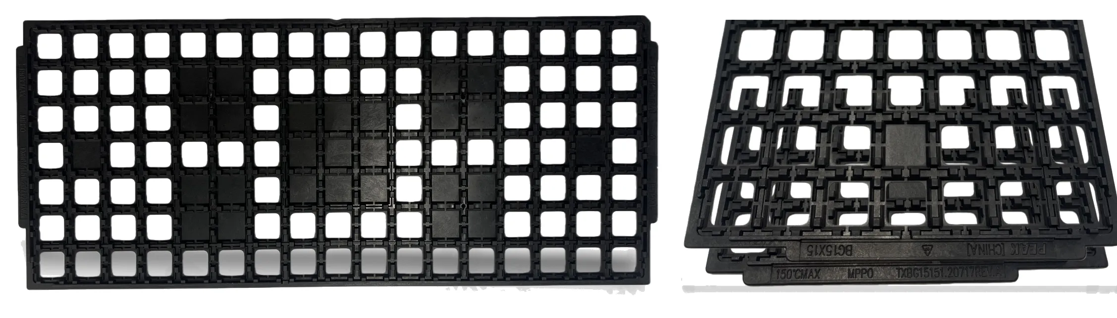
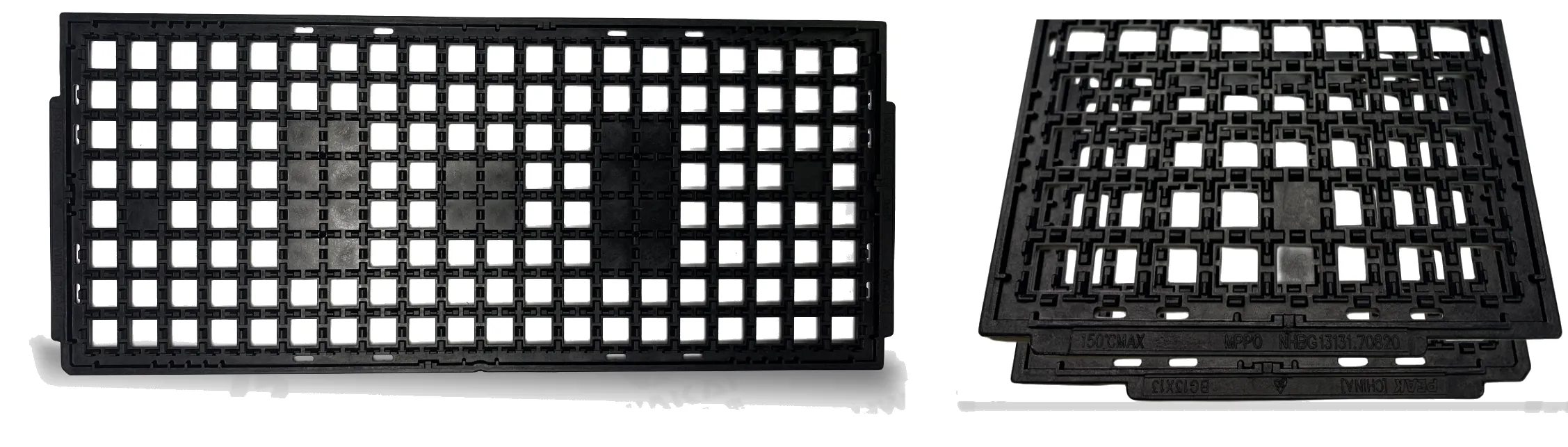
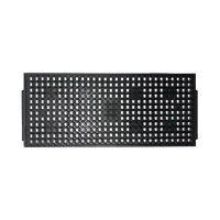
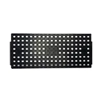
| Productmodel | BGA6x8 | BGA8x8 | BGA11.5×13 | BGA13x13 | |
 |
 |
 |
 |
||
| Specificatieparameters | ●Model | EA70608-10 | NXBG08080.912296REV.A | EA7121321-10 | NHBG13131.70820 |
| ●Tray cavity design | BGA | BGA | BGA | BGA | |
| ●Specifications | 6*8 | 8*8 | 11.5*13*0.8 | 13*13 | |
| ●Matrix | 16*30=480 | 12*29=348 | 8*19=152 | 8*20=160 | |
| ●Temperature MAX (℃) | 150 | 150 | 150 | 150 | |
| ●Surface Resistance | 10^5(Ω)~10^11(Ω) | 10^5(Ω)~10^11(Ω) | 10^5(Ω)~10^11(Ω) | 10^5(Ω)~10^11(Ω) | |
| ●Weight (g) | 138.5 | 162.4 | 125 | 110 | |
| Productnaam | IC-tray | ||
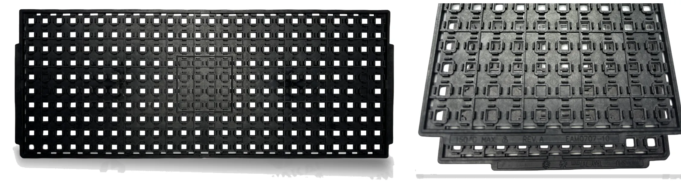
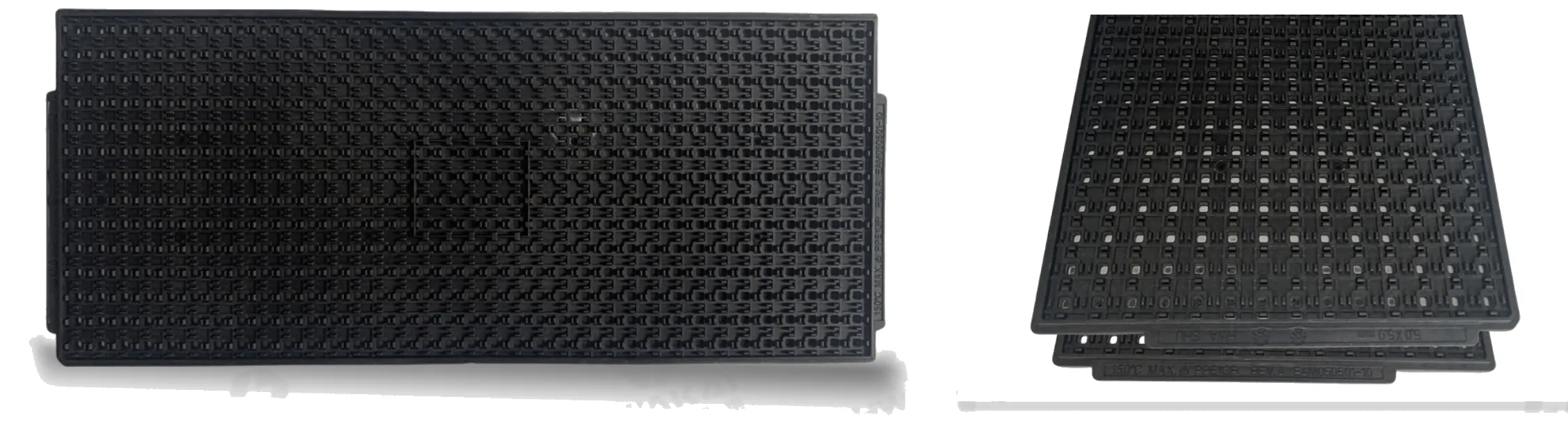
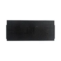
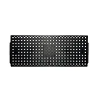
| Productmodel | QFN5x5 | QFN7x7 | |
 |
 |
||
| Specificatieparameters | ●Model | EAM050501-10 | EAM0707-10 |
| ●Tray cavity design | QFN | QFN | |
| ●Specifications | 5*5 | 7*7 | |
| ●Matrix | 14*35=490 | 10*26=260 | |
| ●Temperature MAX (℃) | 150 | 150 | |
| ●Surface Resistance | 10^5(Ω)~10^11(Ω) | 10^4(Ω)~10^11(Ω) | |
| ●Weight (g) | 183.9 | 148 | |
Wereldwijde ESD-productiecapaciteit
Wanneer u inkoopt bij Sanwei, werkt u direct samen met een toonaangevende OEM/ODM-fabrikant. Wij beheren een ultramoderne 70.000+ m² geïntegreerde productiefaciliteit in het Centrale Industriepark van Yueqing, Zhejiang, waarbij elk afzonderlijk proces wordt beheerd, van eigen materiaalformulering tot het uiteindelijke zeer nauwkeurige productvormproces.
Geïntegreerde schaal
70.000+ m² geavanceerde productiefaciliteit, uitgerust met zware precisie-spuitgietmachines om grote wholesalebestellingen te verwerken met stabiele levertijden.
Volledige ketenbeheersing
Volledige beheer in eigen huis, variërend van R&D van eigen antistatisch materiaal, structurele malengineering, geautomatiseerde productie tot snelle wereldwijde logistieke levering.
Grوندige inspectie
Strenge grondstofcontroles in combinatie met meerpuntsmetingen van de oppervlakteweerstand op de productielijn garanderen dat 100% voldoet aan de internationale ESD-richtlijnen.
Antistatisch Producten en Oplossingen
Het leveren van uitgebreide elektrostatische bescherming gedurende uw gehele productie- en operationele levenscyclus.
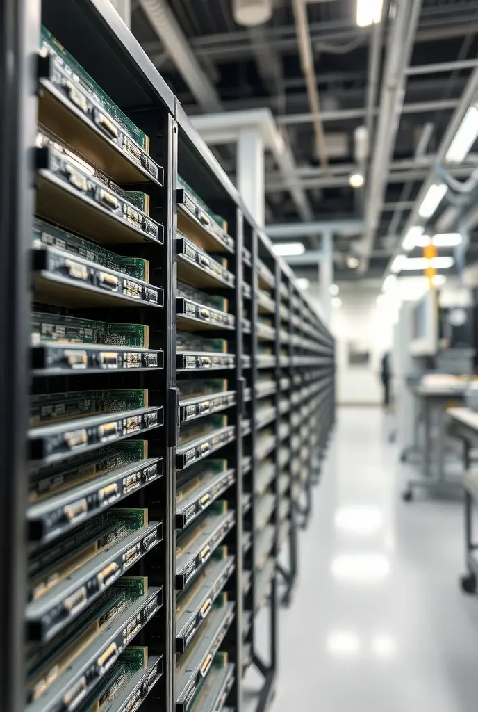
SMT-apparatuur
Antistatische verzamelbakken en rekken voor geautomatiseerde lijnen.

Opslag & Logistiek
Veilingkarren, legborden, bakken, schalen en onderdelenbakken.

Werkplek & PBM
Antistatische stoelen, matten, polsbandjes en persoonlijke bescherming.
Maatwerkontwikkeling
Ontwikkeling van aangepaste matrijzen en speciale antistatische materialen.
ONZE OEM/ODM-VOORDELEN

Geavanceerde R&D & Materiaalinnovatie
Interne ontwikkelde antistatische materialen met nationale uitvindingsoctrooien en hittebestendigheid tot 200℃. Wij vormen niet alleen — we formuleren compounds.

Volledige productiecapaciteit
30.000㎡ fabriek met complete spuitgiet-, granulatie- en ondersteunende verwerkingssystemen voor een stabiele en efficiënte levering.

Volledig op maat gemaakt proces
Materiaalweerstand, kleur, afmetingen, logo, verpakking en certificeringen — aanpasbaar om te voldoen aan IEC61340-5-1, ANSI/ESD S20.20 of militaire normen.

Gecertificeerde Kwaliteit & Wereldwijde Naleving
“Sanwei heeft met succes aangepaste, hittebestendige, schone trays in natuurlijke kleur ontwikkeld voor onze halfgeleidermontagelijn, ter vervanging van geïmporteerde producten, waarmee uitstekende ESD-veiligheid wordt gewaarborgd en aan de hoge reinheidseisen van de werkplaats wordt voldaan.”
BEVERTROUWD DOOR WERELDWIJDE FORTUNE 500 INDUSTRIELEADERS
Onze propriëtaire ESD-oplossingen worden wereldwijd ingezet in geavanceerde productiefaciliteiten, waaronder: Intel, Motorola, Siemens, IBM, Panasonic, Nokia en Dell.
Op zoek naar aangepaste maten of bulk groothandelsprijzen?
Ondersteund door ons robuuste eigen R&D-team biedt Sanwei complete OEM/ODM-opties die zijn afgestemd op uw specifieke SMT-productielijnen of magazijnindeling. Neem vandaag nog contact op met onze specialisten voor aangepaste matrijzen, kleurcodering of geïntegreerd 5S-opslagadvies.
Veelgestelde Vragen (FAQ)
1. What is an IC tray?
It’s basically a plastic tray that holds semiconductor chips during manufacturing, testing, shipping, and storage. They’re specially made to be ESD‑safe so static doesn’t fry the chips. Most of them follow standard sizes so they work with automated handling equipment.
2. What are the materials used in IC packaging?
That’s a whole “package” of stuff – you’ve got the molding compound (usually epoxy resin), a substrate (organic or ceramic), lead frames, die attach adhesives, bonding wires, and solder balls. All these materials work together to protect the chip, connect it to the circuit, and help keep it cool.
3. What material are ice trays made of?
Ice trays for your freezer are a totally different story – they’re all about food safety. The most common are food‑grade polypropylene (PP) and silicone. Silicone’s nice because it’s flexible and makes popping out the ice cubes super easy.
4. What is the standard tray size?
When people say “standard tray,” they usually mean the JEDEC size – that’s 12.7 x 5.35 inches, or about 322.6 x 136 mm. Thickness can be either 0.25 inches (thin) or 0.40 inches (thick). There’s also a common 320mm x 240mm size used internationally.
5. What is a JEDEC tray?
It’s a tray that meets the specs set by JEDEC – the group that writes standards for the semiconductor industry. Think of it as a universal container for chips (like BGA or QFP packages) so that trays from different manufacturers all fit the same machines and processes.
6. What is the tolerance of JEDEC trays?
They’re made to pretty tight tolerances to make sure chips sit exactly right. For example, the dimension accuracy is often around ±0.15 mm, and the overall flatness is kept within about 0.76 mm. That said, the exact numbers can vary a bit between suppliers – always check the data sheet.
7. What is the JEDEC standard?
JEDEC is basically the rule‑maker for the microelectronics world. They publish standards for everything from memory chips (like DDR5) to how parts are packaged and tested. It’s the common language that makes sure chips from different companies can work together.
8. What is the difference between JEDEC and IPC?
Think of it this way: JEDEC focuses on the chip itself – its electrical specs, physical dimensions, and testing. IPC, on the other hand, deals with the circuit board and assembly – how PCBs are designed, manufactured, and soldered. So JEDEC is about the silicon, IPC is about the board.