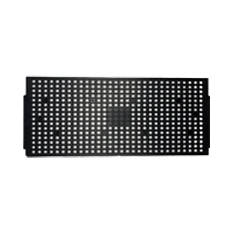
IC Tray JEDEC Standard Anti-Static Chip Packaging Test Tray
Przegląd:
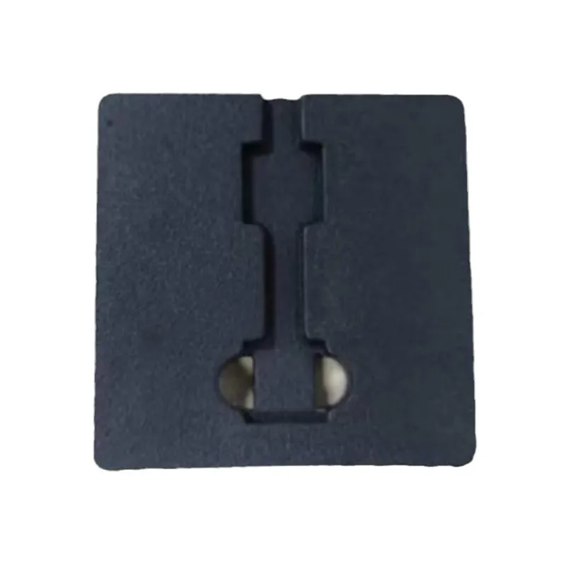
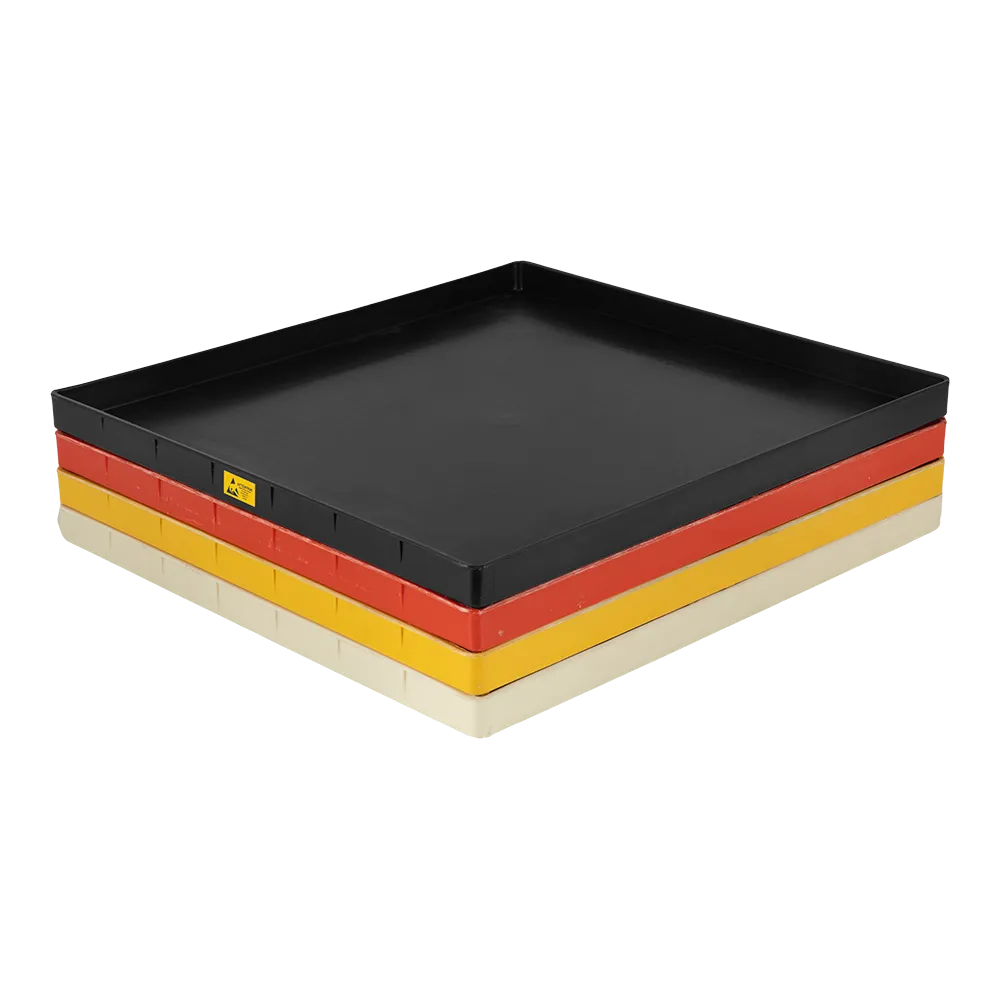
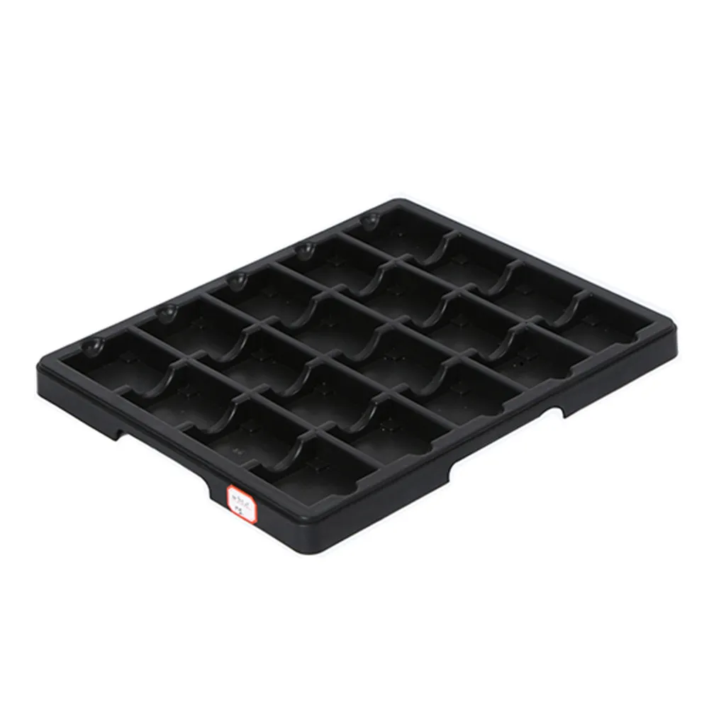
IC tray, also known as electronic chip tray, is a plastic tray used by semiconductor packaging and testing companies for their chip (IC) packaging and testing, complies with JEDEC international standards.
Product Introduction
IC tray, also known as electronic chip tray, is a plastic tray used by semiconductor packaging and testing companies for their chip (IC) packaging and testing, complies with JEDEC international standards.
It can prevent the product from electrostatic contact, protect the chip from damage, and facilitate automated detection and installation. IC trays can be used for various packaging methods such as BGA, QFN, QFP, PGA, TSOP, TQFP, LQFP, PLCC, SOC, SiP, etc.
IC tray material performance requirements
(1) In order to provide electrostatic protection for the chip, the material needs to have antistatic properties, and is generally modified by adding antistatic agents, conductive carbon black or conductive carbon fibers.
(2) Before the chip is assembled at the terminal, it must be baked to avoid moisture inside the chip, which requires the material to be heat-resistant.
(3) The gap between the upper and lower trays needs to hold the pins of the main chip to prevent the pins from shaking and bending or breaking. This requires certain dimensional stability of the material. (4) To avoid the impact of a humid environment on the chip, the tray material is required to have a low water absorption rate.
(5) In order to reduce pollution and save losses, materials are required to be reusable and recyclable.
Technical Specification
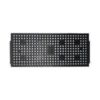
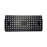
| Product name | IC tray | ||||
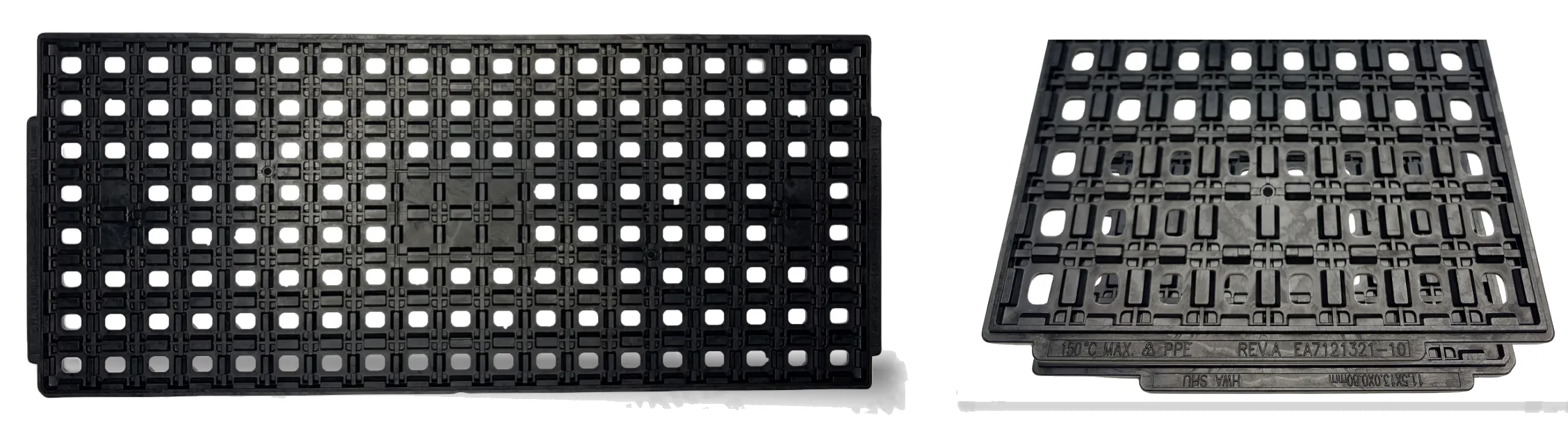
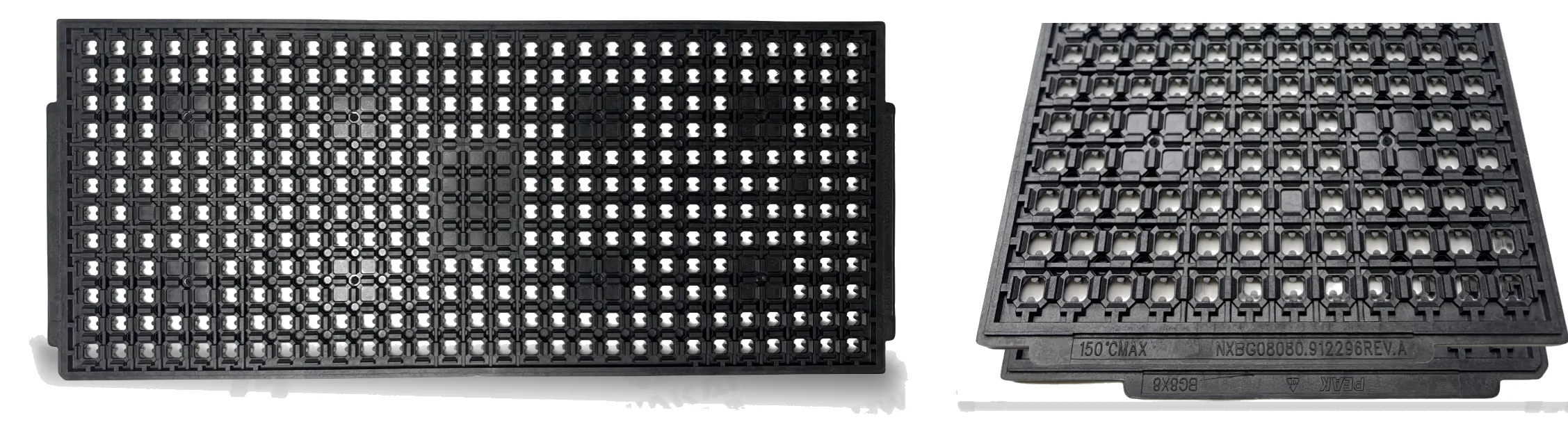
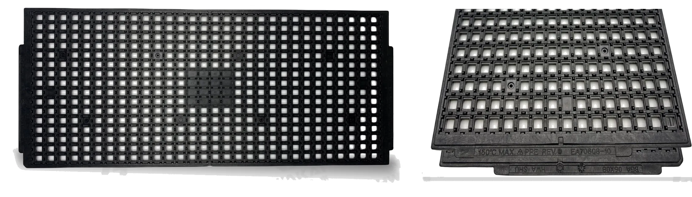
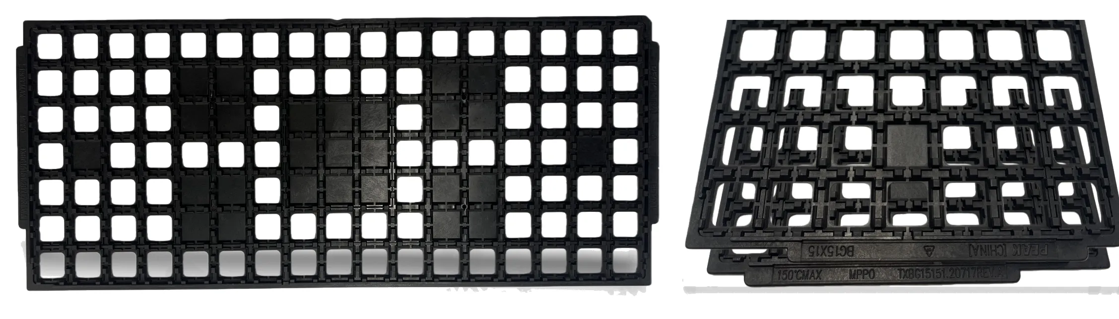
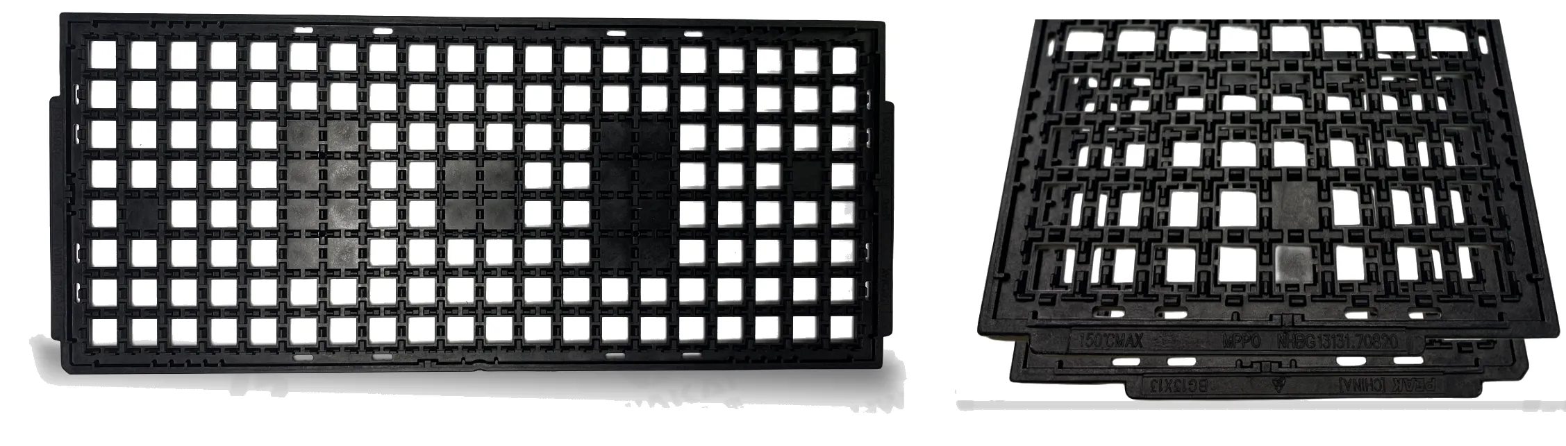
| Product model | BGA6x8 | BGA8x8 | BGA11.5×13 | BGA13x13 | |
 |
 |
 |
 |
||
| Specification parameters | ●Model | EA70608-10 | NXBG08080.912296REV.A | EA7121321-10 | NHBG13131.70820 |
| ●Tray cavity design | BGA | BGA | BGA | BGA | |
| ●Specifications | 6*8 | 8*8 | 11.5*13*0.8 | 13*13 | |
| ●Matrix | 16*30=480 | 12*29=348 | 8*19=152 | 8*20=160 | |
| ●Temperature MAX (℃) | 150 | 150 | 150 | 150 | |
| ●Surface Resistance | 10^5(Ω)~10^11(Ω) | 10^5(Ω)~10^11(Ω) | 10^5(Ω)~10^11(Ω) | 10^5(Ω)~10^11(Ω) | |
| ●Weight (g) | 138.5 | 162.4 | 125 | 110 | |
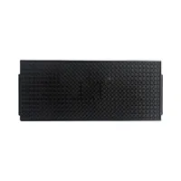
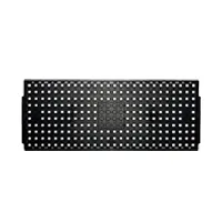
| Product name | IC tray | ||
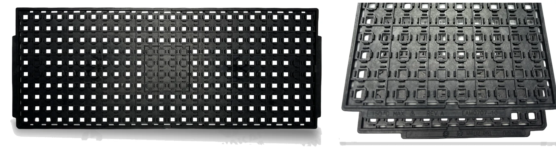
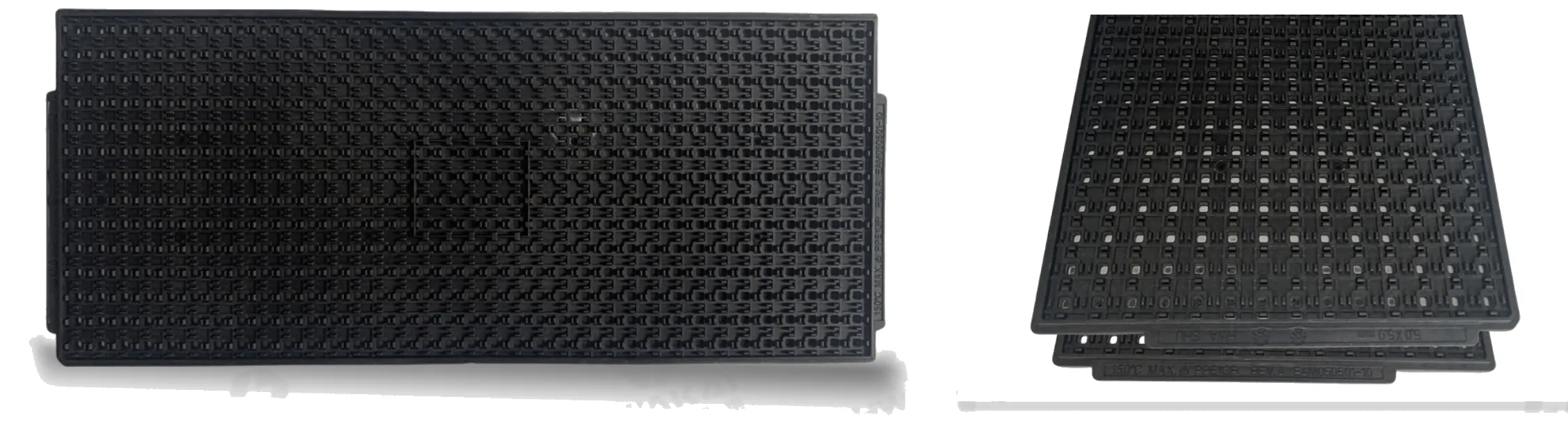
| Product model | QFN5x5 | QFN7x7 | |
 |
 |
||
| Specification parameters | ●Model | EAM050501-10 | EAM0707-10 |
| ●Tray cavity design | QFN | QFN | |
| ●Specifications | 5*5 | 7*7 | |
| ●Matrix | 14*35=490 | 10*26=260 | |
| ●Temperature MAX (℃) | 150 | 150 | |
| ●Surface Resistance | 10^5(Ω)~10^11(Ω) | 10^4(Ω)~10^11(Ω) | |
| ●Weight (g) | 183.9 | 148 | |
Światowej klasy potencjał produkcyjny ESD
Wybierając współpracę z Sanwei, partnerujesz bezpośrednio z wiodącym w branży producentem OEM/ODM. Posiadamy nowoczesne Zintegrowany zakład produkcyjny o powierzchni ponad 70 000 m² w Centralnym Parku Przemysłowym Yueqing w prowincji Zhejiang, zarządzając każdym pojedynczym procesem, od opracowania własnych formulacji materiałowych po ostateczne formowanie produktów o wysokiej precyzji.
Zintegrowana skala
Ponad 70 000 m² nowoczesnego zakładu wyposażonego w wytrzymałe, precyzyjne wtryskarki do obsługi hurtowych zamówień masowych z zachowaniem stabilnych terminów realizacji.
Kontrola całego łańcucha
Pełna kontrola wewnętrzna obejmująca badania i rozwój własnych materiałów antyelektrostatycznych, projektowanie form konstrukcyjnych, zautomatyzowaną produkcję oraz szybką globalną logistykę dostaw.
Rygorystyczna inspekcja
Rygorystyczne badania surowców w połączeniu z wielopunktowym pomiarem rezystywności powierzchniowej na linii produkcyjnej gwarantują zgodność modelu 100% z wytycznymi międzynarodowych norm dotyczących ochrony przed wyładowaniami elektrostatycznymi (ESD).
Antystatyczny Produkty i rozwiązania
Zapewnienie kompleksowej ochrony elektrostatycznej w całym cyklu produkcyjnym i operacyjnym.
Sprzęt SMT
Antystatyczne pojemniki zbiorcze i stojaki do linii zautomatyzowanych.

Magazynowanie i logistyka
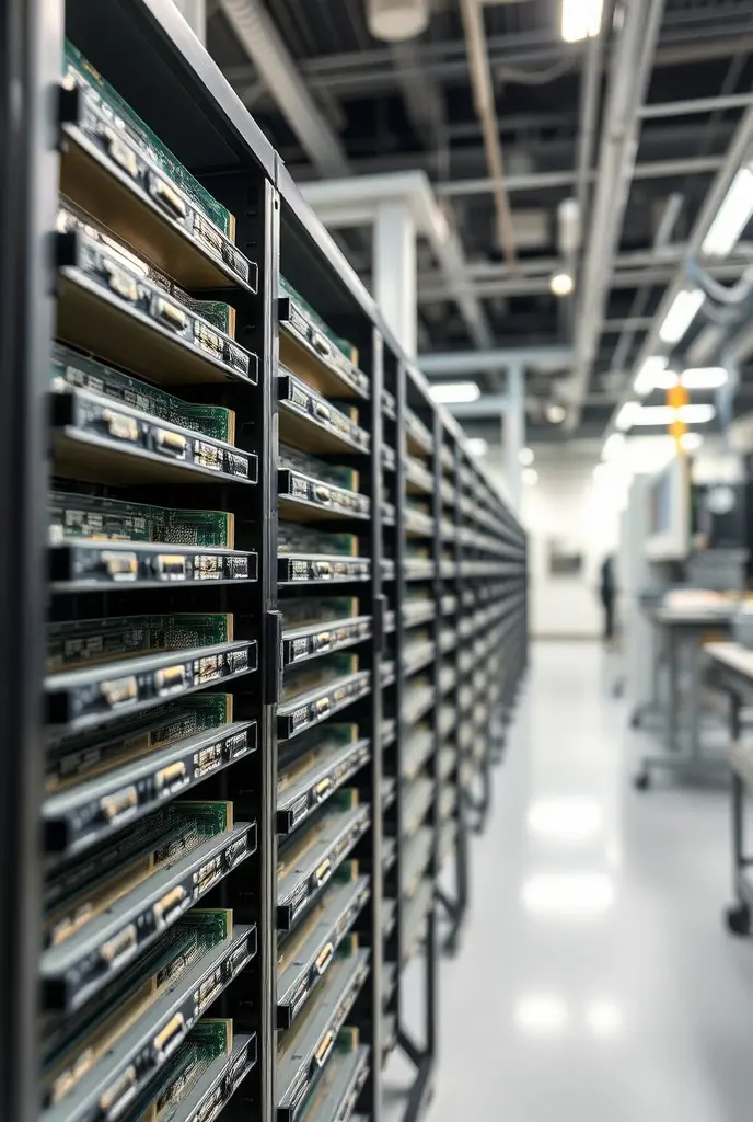
Wózki technologiczne, półki, skrzynie, tace i pojemniki na komponenty.

Stanowisko robocze i ŚOI
Antystatyczne krzesła, maty, paski na nadgarstek oraz ochrona osobista.
Wdrożenia dedykowane
Rozwój niestandardowych form oraz specjalne materiały antystatyczne.
NASZE ZALETY OEM/ODM

Zaawansowane prace B+R i innowacje materiałowe
Własne materiały antystatyczne opracowane wewnątrz firmy, objęte krajowymi patentami na wynalazki i odporne na temperaturę do 200℃. My nie tylko formujemy – my tworzymy związki chemiczne.

Pełnomocna zdolność produkcyjna
Fabryka o powierzchni 30 000 m² z kompletinymi systemami formowania wtryskowego, granulacji i przetwarzania wspomagającego dla zapewnienia stabilnych i wydajnych dostaw.

Kompleksowa personalizacja
Rezystywność materiału, kolor, rozmiar, logo, opakowanie i certyfikaty – możliwość dostosowania do norm IEC61340-5-1, ANSI/ESD S20.20 lub norm wojskowych.

Certyfikowana jakość i globalna zgodność z przepisami
“Firma Sanwei z powodzeniem opracowała niestandardowe, odporne na wysokie temperatury tace o czystym, naturalnym kolorze dla naszej linii montażowej półprzewodników, zastępując produkty importowane, zapewniając doskonałe bezpieczeństwo ESD i spełniając wysokie wymagania dotyczące czystości warsztatu.”
ZAUFALI MIĘDZYNARODOWYM LIDEROM RYNKOWYM Z LISTY FORTUNE 500
Nasze autorskie rozwiązania ESD są wdrażane w elitarnych zakładach produkcyjnych na całym świecie, w tym: Intel, Motorola, Siemens, IBM, Panasonic, Nokia i Dell.
Szukasz niestandardowych rozmiarów lub hurtowych cen?
Wspierani przez nasz silny, wewnętrzny zespół Badawczo-Rozwojowy (R&D), oferujemy kompleksowe opcje OEM/ODM dostosowane do Twoich konkretnych linii produkcyjnych SMT lub układu magazynu. Skontaktuj się z naszymi specjalistami już dziś w sprawie niestandardowych form, kodowania kolorami lub zintegrowanego doradztwa w zakresie magazynowania 5S.
Często zadawane pytania (FAQ)
1. What is an IC tray?
It’s basically a plastic tray that holds semiconductor chips during manufacturing, testing, shipping, and storage. They’re specially made to be ESD‑safe so static doesn’t fry the chips. Most of them follow standard sizes so they work with automated handling equipment.
2. What are the materials used in IC packaging?
That’s a whole “package” of stuff – you’ve got the molding compound (usually epoxy resin), a substrate (organic or ceramic), lead frames, die attach adhesives, bonding wires, and solder balls. All these materials work together to protect the chip, connect it to the circuit, and help keep it cool.
3. What material are ice trays made of?
Ice trays for your freezer are a totally different story – they’re all about food safety. The most common are food‑grade polypropylene (PP) and silicone. Silicone’s nice because it’s flexible and makes popping out the ice cubes super easy.
4. What is the standard tray size?
When people say “standard tray,” they usually mean the JEDEC size – that’s 12.7 x 5.35 inches, or about 322.6 x 136 mm. Thickness can be either 0.25 inches (thin) or 0.40 inches (thick). There’s also a common 320mm x 240mm size used internationally.
5. What is a JEDEC tray?
It’s a tray that meets the specs set by JEDEC – the group that writes standards for the semiconductor industry. Think of it as a universal container for chips (like BGA or QFP packages) so that trays from different manufacturers all fit the same machines and processes.
6. What is the tolerance of JEDEC trays?
They’re made to pretty tight tolerances to make sure chips sit exactly right. For example, the dimension accuracy is often around ±0.15 mm, and the overall flatness is kept within about 0.76 mm. That said, the exact numbers can vary a bit between suppliers – always check the data sheet.
7. What is the JEDEC standard?
JEDEC is basically the rule‑maker for the microelectronics world. They publish standards for everything from memory chips (like DDR5) to how parts are packaged and tested. It’s the common language that makes sure chips from different companies can work together.
8. What is the difference between JEDEC and IPC?
Think of it this way: JEDEC focuses on the chip itself – its electrical specs, physical dimensions, and testing. IPC, on the other hand, deals with the circuit board and assembly – how PCBs are designed, manufactured, and soldered. So JEDEC is about the silicon, IPC is about the board.