- Ханьци
- Блог
Риск одного необнаруженного разряда статического электричества в современной среде производства электроники заключается в том, что дорогостоящая печатная плата не будет работать — возможно, через несколько недель после прохождения окончательной инспекции. Скрытый дефект, который невозможно обнаружить стандартными проверками качества, является одной из наиболее распространенных причин риска надежности для глобальной цепочки поставок электроники. Из-за более высокой плотности, тонких выводов компонентов и более низких рабочих напряжений для печатных плат их чувствительность к электростатическому разряду значительно возросла.
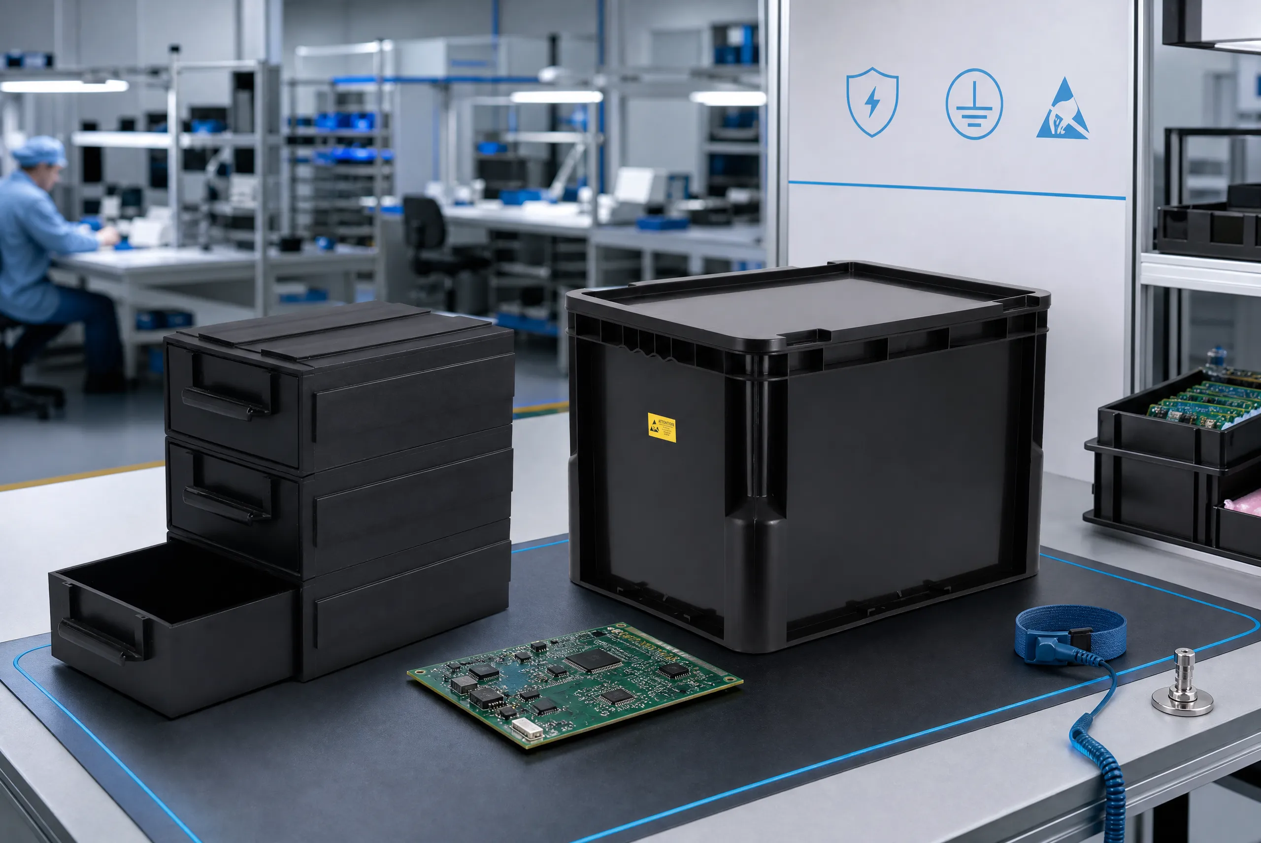
ESD-упаковка — это не просто способ защиты от электростатического разряда (ЭСР), но и комплексная система, разработанная для контроля электростатических эффектов на протяжении всего срока службы изделия, независимо от того, собираете ли вы его на станке SMT, обращаетесь с ним в чистой комнате, отправляете грузовым авиационным или морским транспортом или помещаете на длительное хранение на складе; ESD-упаковка используется на протяжении всего жизненного цикла изделия. В этой статье представлен всесторонний анализ ESD-упаковки с точки зрения данных и технических аспектов для производителей печатных плат; включая типы возможных отказов, принципы работы ESD-упаковки, выбор материалов, международные стандарты ESD-упаковки, риски ЭСР в цепочке поставок и передовые практики закупки материалов, используемых при изготовлении ESD-упаковки.
Понимание упаковки для защиты от электростатического разряда
Упаковка ESD разработана специально для управления электростатическими свойствами печатной платы во время хранения, транспортировки и перемещения.
Стандартные пластики могут как создавать, так и удерживать статический заряд; тогда как ESD-упаковка имеет три основных электрических функции, основанных на её конструкции.
- Рассеяние – безопасное снятие статического заряда с поверхности упаковки с контролируемой скоростью.
- Экранирование – предотвращение проникновения внешних электростатических полей к расположенной внутри печатной плате, выполняя функцию клетки Фарадея.
- Изоляция – Предотвращение накопления трибоэлектрических зарядов, генерируемых трением, между упаковочным материалом и продуктами.
Эти параметры электростатической защиты (поверхностное сопротивление, время распада заряда и эффективность экранирования) обеспечивают достижение поставленных функций — не только за счет механической защиты [т.е. использования полиэтиленового пакета]. Плохо спроектированный полиэтиленовый пакет не обеспечивает существенной защиты от электростатического разряда. Правильно спроектированный экранирующий пакет от электростатического разряда может снизить вероятность электростатического повреждения на несколько порядков по сравнению с неправильно спроектированным. ESD пакет.
Отраслевая перспектива: Более 30% случаев необъяснимых отказов в эксплуатации автомобильной электроники связаны с скрытыми неисправностями, вызванными электростатическим разрядом (EOS/ESD Association, 2022).
Почему защита от электростатического разряда критически важна в цепочках поставок печатных плат
Одной из основных проблем надежности в производстве электроники является электростатический разряд (ЭСР). Наиболее вредоносным видом повреждения от ЭСР является скрытый отказ, который остается внутри и не влияет на непосредственную функциональность в краткосрочной перспективе, а вместо этого приводит к преждевременному отказу из-за термических циклов, механических нагрузок или длительных электрических нагрузок.
Неисправности, возникающие в условиях эксплуатации через несколько месяцев без видимых для пользователя причин, называются скрытыми неисправностями. Ассоциация EOS/ESD сообщает, что на долю скрытых неисправностей, связанных с электростатическим разрядом (ESD), приходится 30% всех возвратов продукции из эксплуатации по необъяснимым причинам; чаще всего это происходит на рынках, где предъявляются высокие требования к надежности.
- Автомобильная электроника – где один неисправный ЭБУ может привести к массовым отзывам.
- Аэрокосмические системы – там, где сбой недопустим, а расходы на выездную техническую поддержку достигают астрономических размеров.
- Промышленные системы управления — где внезапные простои нарушают работу целых производственных линий.
- Полупроводниковая упаковка – где толщина слоёв диэлектрика затвора в современных ИС составляет всего несколько нанометров.
Вот что вам следует знать: устройства, которые исправно работают при прохождении первых тестов и были правильно собраны, по-прежнему подвержены повреждению от электростатического разряда до тех пор, пока на них не повлияют фактические условия эксплуатации. Поэтому обеспечение защиты от электростатического разряда заключается в надежном производстве устройств, а не в логистике их упаковки.
Совет покупателю: При оценке поставщиков печатных плат запрашивайте информацию о соответствии их программы контроля электростатического разряда (ESD) требованиям, предусмотренным ANSI/ESD S20.20 — это наиболее широко признанный отраслевой эталон.
Электростатические механизмы отказа в системах печатных плат
Печатные платы подвержены повреждениям от электростатического разряда (ЭСР) из-за ряда установленных механизмов, каждый из которых должен быть понят инженерами для принятия обоснованных решений о соответствующей упаковке и обращении.
1. Скрытое повреждение от электростатического разряда
Когда электростатический разряд (ESD) вызывает появление микроскопических дефектов в полупроводниковых переходах или оксидах затвора, происходит внутреннее разрушение диэлектрика. Хотя эти дефекты не приводят к мгновенному выходу устройства из строя, они ослабляют его. Со временем устройство может выйти из строя в результате термоциклирования, механической вибрации или электрической нагрузки, действующей на ослабленную область. В большинстве случаев скрытые повреждения не выявляются при проведении стандартных электрических испытаний; поэтому именно они являются причиной многих отказов в эксплуатации, связанных с электростатическим разрядом.
2. Трибоэлектризация
Когда два предмета соприкасаются друг с другом и затем разделяются, электроны передаются с одной поверхности на другую, в результате чего возникает электрический заряд, который остается после разделения предметов. Этот процесс наиболее часто происходит при работе с печатными платами (ПП) и может возникать, когда компоненты скользят по полимерным лоткам, снимается защитная статическая пленка с оголенной ПП или во время вращения катушек на установщике поверхностного монтажа (SMT). Подавляющее большинство событий электростатического разряда (ЭСР) в автоматизированном производстве происходит из-за трибоэлектрического заряда (трение).
3. Влияние влажности окружающей среды
Уровень влажности влияет на то, насколько быстро можно удалить статические заряды с поверхностей; поэтому, если относительная влажность опускается ниже 30%, скорость удаления зарядов значительно снижается, а статические заряды могут достигать нескольких тысяч вольт. Такие уровни заряда в воздухе могут быть особенно опасны при перевозке грузов по воздуху; влажность в салоне самолета на высоте может быть ниже 10%, равно как и в зимний период на складах в регионах с холодным климатом.
Таблица 1: Сравнение механизмов отказа вследствие электростатического разряда
| Тип сбоя | Механизм | Видимость | Тайминг | Уровень риска |
|---|---|---|---|---|
| Скрытый сбой | Деградация диэлектрика | Invisible | Delayed | Very High |
| Catastrophic Failure | Direct discharge breakdown | Visible | Immediate | Critical |
| Triboelectric Charging | Frictional charge buildup | Invisible | Handling stage | Высоко |
| Humidity-Driven Charging | Reduced charge dissipation | Invisible | Environmental | Высоко |
Отраслевая перспектива: Catastrophic failures—those that cause immediate visible damage—represent only 10 to 20 percent of all ESD events. The vast majority are latent, slipping through standard quality assurance inspections.
Engineering Principles of ESD Packaging
The basic components of modern Упаковка для защиты от электростатического разряда are based on a multilayered electrostatic control architecture. Although the designs will vary depending on their intended use, the basic structure will have three primary functional layers.
- Dissipative layer – Generally speaking, an inner surface with defined conductive material (10^6ceDitto 10^*0Dorrnit &0.^0Z) allowing for safe or gradual discharge.
- Conductive layer Electric charge is distributed over the surface of a large area by way of a conductor that has been buried within a dielectric insulator: the result is a near-zero potential difference between points on the conductor.
- Shielding layer Generally, a metal layer (aluminum deposited on polyester) that functions as a Faraday cage and prevents external electrostatic fields from affecting the enclosed PCB.
With its three-layer structure, this design provides both internal charge control (but prevents any accumulation of charged particles as a result of triboelectric effect) and shielding from external electric fields (preventing damage to components by nearby electrical sources). The three-layered design is an absolute must for any device that contains extremely sensitive components, e.g., sophisticated ICs, RF modules, or MEMS sensors.
Key Performance Parameters
The selection of ESD packaging is based on the qualification of ESD packaging using measurable electrical properties. The table below summarizes the specifications that are most critical and defined by industry standards.
| Параметр | Typical Range | Функция | Engineering Role |
|---|---|---|---|
| Surface Resistivity | 10⁶–10¹¹ Ω/sq | Charge dissipation | Prevents static charge buildup on packaging surfaces |
| Charge Decay Time | < 2 seconds | Discharge speed | Ensures rapid neutralization of accumulated charge |
| Shielding Effectiveness | > 40 dB | Field blocking | Reduces external ESD energy to safe levels for ICs |
| Humidity Stability | 20%–80% RH | Environmental adaptability | Maintains performance across real-world logistics conditions |
| Thermal Resistance | up to 160–200°C | High-temperature tolerance | Enables compatibility with SMT reflow and baking processes |
The charge decay time test evaluates the time required for an initial voltage (usually +/- 1000 volts) to decay to a value of 10% of the original voltage to measure the ability of material to dissipate a charge. According to IEC 61340-5-1, a requirement will be met if the measured charge decay time is greater than or equal to two seconds. If the range of surface resistivity on a material is in the dissipative region, but the measured charge decay time is greater than two seconds, the material may not be appropriate for use.
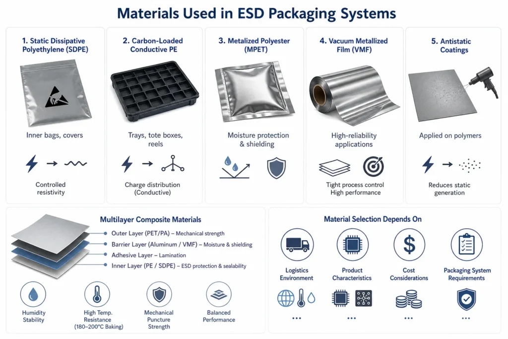
Materials Used in ESD Packaging Systems
ESD packaging materials consist of engineered composites, which are carefully selected based on their unique properties (e.g. electrical, mechanical and thermal) to meet specific needs. Examples of commonly used materials in ESD packaging include:
- Static dissipative polyethylene (SDPE) – a flexible film with controlled resistivity, used for inner bags and covers.
- Carbon-loaded conductive polyethylene – used for trays, tote boxes, and component reels where charge distribution is needed.
- Metalized polyester (MPET) – A thin aluminum layer is deposited on a PET film so that it can provide moisture protection and shielding. I often use polyethylene, which means it is usually used in multilayer foil packaging bags.
- Vacuum metallized film (VMF) – similar to MPET but with tighter process control, often used for high-reliability applications.
- Antistatic coatings – topical coatings applied directly to polymers to decrease generation of static electricity (though generally not as durable as built-in dissipative products).
Multilayer composite materials are developed by combining materials into advanced package systems that provide balanced performance characteristics of humidity stability, high temperature resistance (baking up to temperatures of approximately 180 – 200 degrees celcius) and mechanical puncture strength. Material selection will vary according to the attributes of the packaging system in relation to the particular logistics environment, the characteristics of the product being packaged, and costs considerations.
Manufacturing and International Standards
ESD packaging manufacture is a controlled polymer engineering process. Key steps include:
- Polymer compounding – Mixing Carbon black, carbon nanotubes, graphene or conductive fillers with the base resin or adding antistatic additives to base resin.
- Extrusion under controlled humidity – ensuring consistent dispersion and surface properties.
- Metallization or coating – depositing thin metal layers via vacuum evaporation or sputtering.
- Multilayer lamination – combining functional layers with adhesives to maintain integrity under flexing and heat.
- Heat sealing and forming – converting film into bags, pouches, or rigid trays.
All ESD packaging should comply with established international standards:
| Стандарт | Scope |
|---|---|
| IEC 61340-5-1 | Electrostatic control systems for electronics; the global reference |
| ANSI/ESD S20.20 | ESD control program requirements; widely adopted in North America |
| IPC-1601 | PCB handling and storage guidelines; covers ESD packaging as part of process control |
| RoHS | Restriction of hazardous substances; environmental compliance |
Отраслевая перспектива: Over 80% of tier-1 electronics manufacturing service (EMS) providers require their packaging suppliers to hold certification for both IEC 61340-5-1 and ANSI/ESD S20.20 to ensure global compliance.
ESD Packaging in PCB Supply Chains
Electronic discharge (ESD) risks extend beyond just factories. Electrical discharges (ESD) pose a risk across the entirety of the worldwide logistics chain. The amount of risk associated with electrical discharges (ESD) is dependent on one’s location.
| Environment | Уровень риска | Main Source | Recommended Packaging |
|---|---|---|---|
| SMT Production Line | Высоко | Machine friction, operator handling | Multilayer shielding bags or bins |
| Air Freight | Very High | Low humidity (can fall below 10% RH at altitude) | Metallized shielding film with moisture barrier |
| Warehouse Storage | Medium | Charge accumulation on surfaces | Dissipative bags or covers |
| Cleanroom | Высоко | Human contact, synthetic garments | Full ESD-protective packaging (bags, boxes, labels) |
| Ocean Shipping | Medium | Temperature and humidity cycles | Moisture-stable composite materials |
Air freight purchasers should request metallized shielding film with shielding effectiveness higher than 40 dB and also have a built-in moisture barrier. Because there is a very low level of humidity and there is a rapid pressure drop while climbing in altitude, there is an additional potential for generating ESD in the air freight environment.
Procurement Guide for ESD Packaging
Choosing a suitable ESD packaging supplier cannot be accomplished solely based on price; engineering performance is another factor to consider. When conducting the technical audit, the following criteria can be included:
- IEC / ANSI compliance certification – verified by an independent third-party (SGS, TÜV, etc.).
- Shielding effectiveness data – measured per IEC 61340-5-1 or ANSI/ESD STM11.31.
- Charge decay test reports – showing < 2 seconds decay time under stated temperature and humidity conditions.
- Humidity and temperature stability – performance curves across the expected logistics range (e.g., 20%–80% RH).
- OEM/ODM capability – ability to custom-design packaging geometry, material selection, and printing.
- Batch-to-batch consistency – internal quality control data showing CPK values above 1.33 for key parameters.
Отраслевая перспектива: Cost-driven selection of ESD packaging—without engineering validation—has been directly linked to a 5–8% increase in field failure rates among semiconductor packagers. Leading companies now require incoming quality control (IQC) testing on every lot.
Часто задаваемые вопросы
Q1: What is ESD packaging for PCB used for?
Q2: Do PCBs really need ESD packaging?
Q3: Why do PCBs still fail after ESD packaging?
Q4: What is the best packaging for PCB shipping?
Q5: What should buyers check before choosing suppliers?
Q6: Can standard pink‑poly antistatic bags provide adequate protection?
Q7: How often should ESD packaging be requalified?
Q8: Is there a difference between “static dissipative” and “conductive” packaging?
ESD packaging for PCB manufacturers is a technical discipline grounded in electrical engineering, materials science, and standards compliance. It is not an accessory—it is a critical component of the overall reliability assurance system for electronic products. From understanding failure mechanisms and multilayer design principles to selecting materials and qualifying suppliers against IEC and ANSI standards, every decision matters.
For procurement and engineering teams, the takeaway is clear: treat ESD packaging as an engineered reliability solution, not a commodity. Invest in supplier verification, performance testing, and logistics-specific design. The cost of doing so is small compared to the field failure exposure that latent ESD damage can cause—especially in automotive, aerospace, and industrial applications where reliability is paramount.
By applying the principles and data outlined in this guide, buyers and engineers can significantly reduce ESD-related risks and build a more resilient electronics supply chain.
Ссылки
- IEC 61340-5-1: Electrostatic Control Standard – International Electrotechnical Commission. https://webstore.iec.ch/en/publication/74748
- ANSI/ESD S20.20: ESD Control Program Standard – EOS/ESD Association. https://www.esda.org
- IPC-1601: PCB Handling and Storage Guidelines – IPC. https://www.ipc.org
- EOS/ESD Association Technical Publications. https://www.esda.org
- MarketsandMarkets. “Electronics Packaging Market Report” (2023). https://www.marketsandmarkets.com


Оставить ответ