- Ханьци
- Блог
The semiconductor industry is moving into a new stage of rapid progress caused by the growing consumption of chips for AI, car electronics, 5G appliances, and powerful computing systems. The sizes, complexity, and sensitivity of IC components increase which creates more demands for its handling, storages, and transportation.
With new technologies like BGA, CSP, QFN, and wafer-level packaging being introduced, traditional packaging approaches fail to deliver the accuracy needed in positioning, cleaning, and automation. Semiconductor companies have begun to make use of specialized ESD trays that ensure anti-static handling because of the need for better packaging solutions.
Buyers have to know that choosing the right ESD tray is not just packaging: it is an essential factor influencing product quality, manufacturing efficiency, and production costs. Yet, lots of companies still have doubts about selecting the supplier due to such issues as inconsistent resistivity, poor dimensional accuracy, lack of customization, and suitability for the semiconductor industry.
A dependable thermoformed ESD tray maker who possesses robust input control over the materials utilized in the manufacturing process, proven engineering methodologies, and mastery of the custom fabrication technique will certainly assist semiconductor companies achieve risk reduction and improve their packaging performance.
What Is ESD Protection?
In the electronic assembly as well as semiconductor manufacturing, Защита от ЭСД also referred to as Electrostatic Discharge Protection involves a set of technologies and processes meant to ensure prevention of damage caused by sudden electrostatic discharges. During transportation, production as well as handling, static electricity may be encountered, which in turn results in generation of very high transient voltages capable of causing damage to sensitive electronic components.
While mechanical damage can be noticed by visual inspection, ESD is often hidden and causes latent failures. Thus, ESD control plays an important role in all parts of the semiconductor supply chain, especially during IC packaging, testing, storage, and shipping.
What Are Thermoformed ESD Trays for IC Packaging?
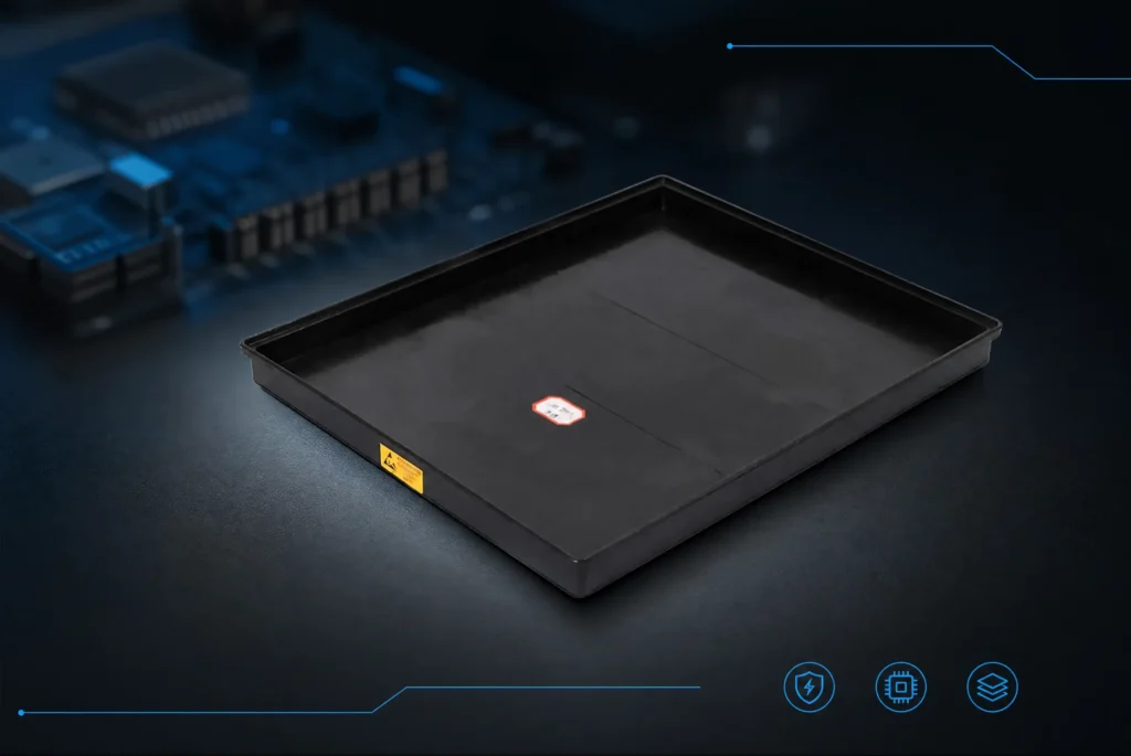
A specific carrier in the semiconductor industry, ESD thermoform tray is made from static controlled material through the process of thermoforming. The primary purpose of the ESD trays is to keep the electronic devices secure from any external damage and other environmental hazards.
In contrast to traditional plastic trays, which can build up static electricity charges, ESD trays are designed to have anti-static, dissipative, or conductive qualities in order to eliminate any electrostatic charges from the components placed inside.
Manufacturers utilize the thermoforming process in order to make tray design based on specific IC packages dimensions, such as the pocket geometry, cavity depth, orientation of the components and loading conditions.
A typical custom thermoformed ESD tray consists of:
- Multiple precision cavities for IC placement
- ESD-controlled plastic substrate
- Robotic handling features
- Stackable tray structures
- Barcode or identification areas
- Cleanroom-compatible surfaces
Materials Used for Anti Static IC Trays
The electrical performance, mechanical strength, and applicability for semiconductor usages of an anti static IC tray are determined by the choice of material.
Various semiconductor packaging conditions necessitate different material characteristics such as surface resistivity, stability, chemical resistivity, and heat resistance.
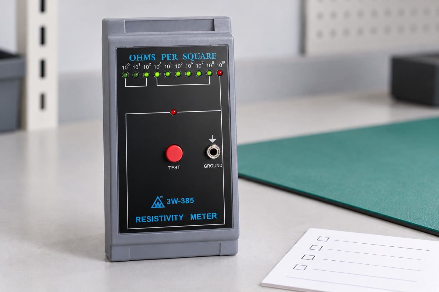
Surface Resistance: Surface Resistance is a determination of the opposition that a material shows to the conduction of electricity across its exterior area and often is utilized in the assessment of the electrostatic discharges’ performance.
Thermoplastics typically employed for ESD trays include PET, PP, PS, ABS, and carbon-filled polymers.
| Материал | Key Characteristics | Typical Applications |
| ESD PET (Polyethylene Terephthalate) | Excellent dimensional stability, lightweight, good transparency | IC packaging, electronic component transportation |
| ESD PP (Polypropylene) | High chemical resistance, durable, suitable for repeated handling | Semiconductor production lines, reusable trays |
| Conductive ABS | Strong mechanical strength and impact resistance | High-value semiconductor components |
| Carbon-filled plastic | Stable conductivity and excellent ESD control | Advanced IC packaging and precision electronics |
| Static dissipative PS | Cost-effective and suitable for disposable applications | General electronic component packaging |
ESD Tray Electrical Performance: Resistance Values and Testing Standards
Electrical performance is one of the most important factors when evaluating an ESD tray supplier.
A top-grade ESD tray must be characterized by stable electrical resistance properties which can avoid static charge accumulation and discharge.
Mechanical and electrical classifications of ESD materials are important to establish and they are primarily based on the measurements of surface and volume resistances.
Volume resistance refers to the resistance of a given material through its thickness and helps in the evaluation of its electrical conductivity properties.
Thermoformed ESD Trays Vs Injection Molded Trays: Which Is Better?
Thermoformed ESD trays, as well as injection molded trays are extremely popular in packaging of semiconductors, but they have a set of benefits based on the needs of the application.
The process of manufacturing thermoformed trays involves heating plastic sheets followed by molding them on specially designed molds, whereas injection molded trays are created by injecting hot molten plastic through precision molds.
| Сравнительный фактор | Thermoformed ESD Tray | Injection Molded ESD Tray |
| Tooling Cost | Lower initial investment | Higher tooling cost |
| Development Speed | Faster prototype development | Longer development cycle |
| Customization Flexibility | Excellent for customized designs | Better for high-volume standardized products |
| Production Volume | Small to medium batches | Large-scale mass production |
| Dimensional Precision | Высоко | Very high |
| Cost Efficiency | Better for customized IC packaging | Better for very high-volume production |
ESD Tray Design Considerations for Different IC Packages
C packaging keeps changing quickly, imposing new requirements on the design of semiconductor carriers.
ESD tray design should be done while keeping in mind all the parameters related to the components such as size, the needs for handling processes, automation, and safety during transportation process.
Important design factors include
- Pocket Geometry
- IC Package Compatibility
- Automation Compatibility
- Stackability and Transportation Safety
Common Problems with Poor-Quality ESD Trays
Integrating substandard ESD-лотки can lead to critical risks during the semiconductor fabrication process.
While affordable trays may provide savings at the outset, they may also end up causing component damage, operational losses and increased failure rates.
Common problems include:
- Unstable ESD Performance
- Poor Dimensional Accuracy
- Material Deformation
- Surface Contamination
- Lack of Quality Certification
OEM and ODM Customization Options for ESD Packaging Solutions
Requirements for semiconductor packaging may vary widely depending on component design, manufacturing method, and automated machinery used. Hence, the ability to offer customized solutions for the ESD trays is of utmost importance in choosing a supplier of this specific product.
In addition to offering OEM services, manufacturers also provide ODM services using customer specifications as the basis for their solutions.
- Custom engineering drawings
- Product structure development
- Material selection according to application requirements
- Logo and nameplate customization
- Packaging customization
- Настройка цвета
- Instruction manual customization
In the case of IC packaging in particular, customization can include modifications to the tray size and shape, cavity design, location of components on the trays, and certain other specifications applying to the design in order to be compatible with automated manufacturing processes. Suppliers will usually start working with customers during the first stages of their production process, including prototype testing, as well as tests of materials, and samples on the last stage. The services from Sanwei have already passed testing in accordance with internationally accepted standards, including requirements of IEC 61340-5-1, ANSI/ESD S20.20, SGS tests, and RoHS requirements.
Considerations for RoHS: Compliance with RoHS involves meeting the limitations on hazardous materials now expected by legislation that is primarily based on the RoHS directive in the European Union.
Часто задаваемые вопросы
1. What is the difference between an ESD tray and a standard plastic tray?
Поддон для электростатического разряда изготавливается из материалов с контролем статического электричества, чтобы предотвратить накопление статического электричества и обеспечить надлежащую электрическую нейтрализацию. Как правило, пластиковые поддоны не обладают свойствами электропроводности и поэтому небезопасны для обращения с электронными устройствами.
2. What materials are commonly used for ESD trays?
Распространенные материалы включают ESD ПЭТ, ESD ПП, проводящий АБС, полимеры на основе углерода, а также другие композитные антистатические материалы. Требуемое количество будет зависеть от степени необходимого сопротивления, а также от характера температуры, механической прочности и области применения.
3. Can ESD trays be customized according to IC package dimensions?
Действительно, индивидуальные ESD-лотки могут быть созданы в соответствии со спецификациями этих компонентов, включая такие параметры, как размеры ячеек, дизайн лотка, схемы загрузки и требования к автоматизации, среди прочих. Благодаря услугам OEM и ODM производители могут создавать индивидуальные решения для различных корпусов ИС и их производственных процессов.
4. What ESD standards should semiconductor packaging trays comply with?
Standards which are regularly cited include IEC 61340-5-1 and ANSI/ESD S20.20. Further testing relative to customers’ requirements may entail testing like SGS verification while RoHS compliance tests can also be done as part of application-specific qualification tests.
5. How do I choose between thermoformed and injection molded ESD trays?
Термоформованные лотки обычно используются для уникальных спецификаций, быстрой разработки дизайна и гибких производственных процессов. Литьевые лотки чаще применяются для больших объемов производства, где требуется стабильная структура.
6. Can ESD trays withstand high-temperature environments?
Действительно, это основано на проведенном процессе выбора материалов. Некоторые антистатические композитные материалы способны выдерживать температуру либо 160 °C, либо 200 °C, что позволяет использовать их в различных промышленных применениях.
Ссылки
ANSI/ESD S20.20 – Protection of Electrical and Electronic Parts, Assemblies and Equipment
https://www.esda.org/
IEC 61340-5-1 – Electrostatics: Protection of Electronic Devices from Electrostatic Phenomena
https://www.iec.ch/
ESD Handbook ESD TR20.20 – Electrostatic Discharge Control Program Development
https://www.esda.org/
Semiconductor Industry Association (SIA) – Semiconductor Industry Reports
https://www.semiconductors.org/


Оставить ответ