- هانكي
- مدونة
The risk of a single undetected ESD event within a modern electronics manufacturing environment is that a high-value printed circuit board will not work—possibly several weeks after passing final inspection. The latent failure that is not able to be detected through standard quality checks is one of the most common causes of reliability risk for the global electronics supply chain. Due to higher density, finer pitch components and lower operating voltages for PCBs, their susceptibility to electrostatic discharge has increased significantly.
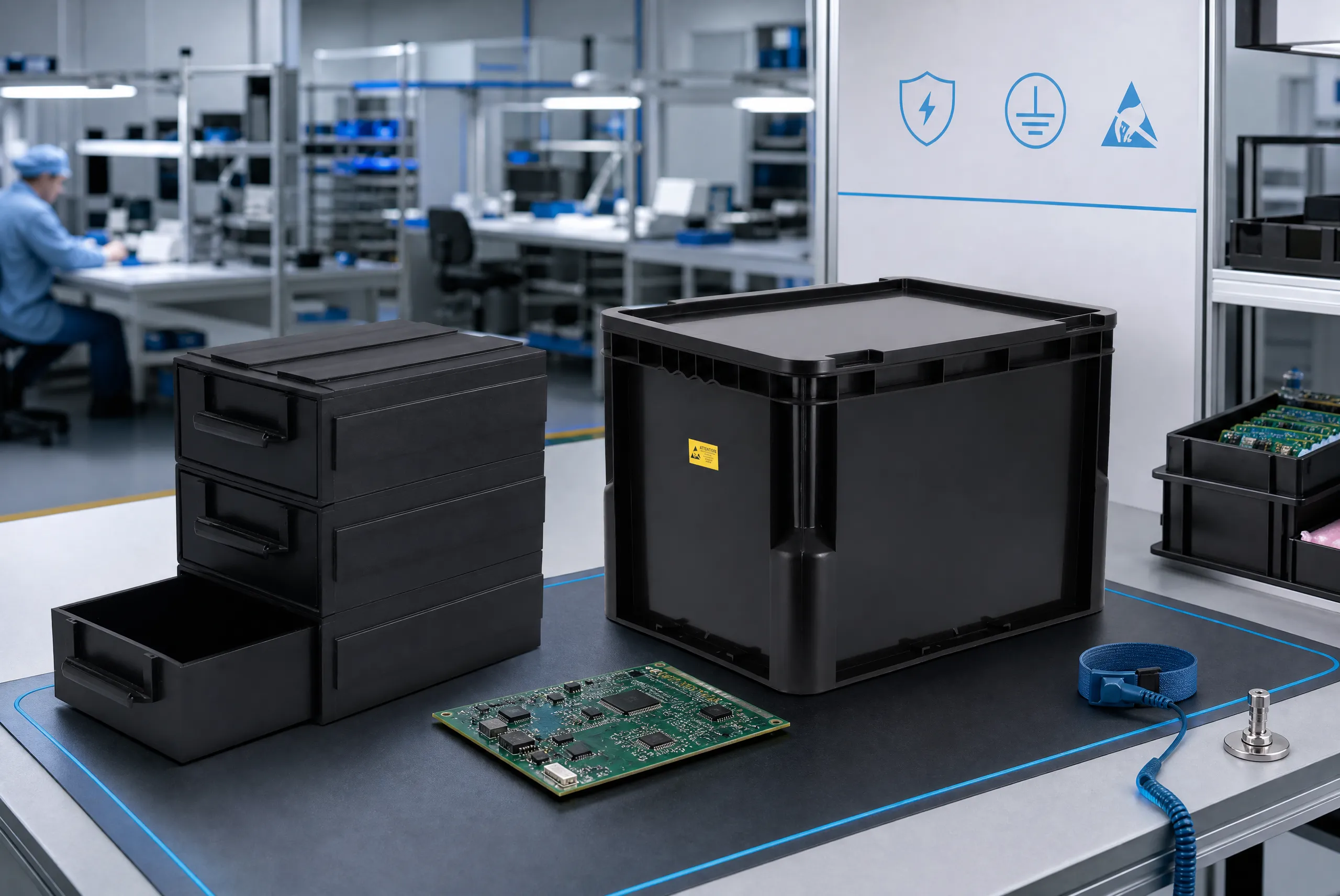
Not just a way to protect from ESD, ESD packaging is also a complete system engineered to control electrostatic effects throughout the life of the product regardless of whether you are building it on your SMT machine, handling it in a clean room, shipping using air freight or ocean freight or putting in long-term storage at a warehouse; ESD packaging has been used throughout the product life cycle. This article presents a comprehensive evaluation of ESD packaging from a data and technical standpoint for PCB manufacturers; including the types of failures that can occur, the engineering principles of how ESD packaging works, selection of materials, international ESD packaging standards, ESD risks in the supply chain and best practices for procuring materials used in making ESD packaging.
Understanding ESD Packaging
ESD Packaging is design specifically to manage the electrostatic properties of a PCB while sitting / stored / in transit.
Standard plastics can both create and hold a static charge; whereas, ESD packaging has three principle electrical functions based on its design.
- Dissipation – safely releasing static charge from the surface of the packaging at a controlled rate.
- Shielding – blocking external electrostatic fields from reaching the enclosed PCB, acting as a Faraday cage.
- Isolation – Preventing friction-generated triboelectric charges from building up between the packaging material and the products.
These electrical performance parameters (surface resistivity, charge decay time, and shielding effectiveness) achieve the functions sought after—not through mechanical protection exclusively [i.e., by using the polyethylene bag]. With a poorly designed polyethylene bag there is no significant protection from ESD. A properly designed ESD shielding bag can reduce the likelihood of electrostatic damage by several magnitudes when compared to an improperly designed ESD shielding bag.
Industry Insight: More than 30% of unexplained field returns in automotive electronics are linked to ESD-related latent failures (EOS/ESD Association, 2022).
Why ESD Protection Is Critical in PCB Supply Chains
One of the main reliability concerns for electronic manufacturing comes from Electro-Static Discharge (ESD). The most impairing kind of ESD damage is latent failure, hiding inside and having no short term failure to impact immediate functionality, but instead resulting in premature failure due to thermal cycling, mechanical stresses, or extended electrical loading.
Field failures that show up months later without any cause of failure visible to the user are called latent field failures. The EOS/ESD Association reports that ESD-related latent failure accounts for 30% of all returns from the field for unexplained reasons; this occurs more often in high-reliability markets.
- Automotive electronics – where a single faulty ECU can trigger recalls at massive scale.
- Aerospace systems – where failure is not an option and field service costs are astronomical.
- Industrial control systems – where unexpected downtime disrupts entire production lines.
- Semiconductor packaging – where advanced ICs have gate oxide layers only a few nanometers thick.
Here’s what you should know: devices that are working properly when they pass the first tests and have been assembled properly are still susceptible to damage from ESD until they are subjected to the stress of actual use. That’s why providing ESD protection is all about building devices reliably, and not about the logistics of packaging them.
Buyer Tip: When evaluating PCB suppliers, request their ESD control program compliance per ANSI/ESD S20.20 — this is the most widely accepted industry benchmark.
Electrostatic Failure Mechanisms in PCB Systems
PCB environments suffer from ESD damage due to a number of established mechanisms, each of which must be understood by engineers to make informed choices about the appropriate packaging and handling.
1. Latent ESD Damage
When an ESD event causes microscopic defects in semiconductor junctions or gate oxides, internal dielectric degradation will occur. While these defects will not instantaneously destroy the device, they will weaken it. Over time, the device may experience failure from heat cycling, mechanical vibration, or electrical stress applied to the weakened region. Most of the time, latent damage is not visible through regular electrical testing; therefore, latent damage is the cause of many ESD-related field failures.
2. Triboelectric Charging
When two items come into contact with one another and separate from one another, electrons are transferred from one of the surfaces to the other surface resulting in the generation of an electric charge that remains when the items are separated. This process occurs most frequently in handling of PCBs (printed circuit boards) and can occur when components slide across polymer trays, peel the static protection layer from the bare PCB, or during rotation of the reels on a (SMT) surface mounted technology pick and place operation. The vast majority of electrostatic discharge (ESD) events in automated production are due to triboelectric charging (frictional).
3. Environmental Humidity Effects
The level of humidity affects how quickly you can remove static electric charges from surfaces very quickly, so if the relative humidity falls below 30% the speed with which you can remove any charge is greatly affected and static electric charges have the potential to be many thousands of volts. These levels of charge in the air can be especially dangerous in air cargo; the humidity in the cabin of an aircraft at altitude can be less than 10%, as well as in cold-climate warehouses in the winter.
Table 1: Comparison of ESD Failure Mechanisms
| Failure Type | Mechanism | Visibility | Timing | Risk Level |
|---|---|---|---|---|
| Latent Failure | Dielectric degradation | Invisible | Delayed | Very High |
| Catastrophic Failure | Direct discharge breakdown | Visible | Immediate | Critical |
| Triboelectric Charging | Frictional charge buildup | Invisible | Handling stage | عالٍ |
| Humidity-Driven Charging | Reduced charge dissipation | Invisible | Environmental | عالٍ |
Industry Insight: Catastrophic failures—those that cause immediate visible damage—represent only 10 to 20 percent of all ESD events. The vast majority are latent, slipping through standard quality assurance inspections.
Engineering Principles of ESD Packaging
The basic components of modern تغليف ESD are based on a multilayered electrostatic control architecture. Although the designs will vary depending on their intended use, the basic structure will have three primary functional layers.
- Dissipative layer – Generally speaking, an inner surface with defined conductive material (10^6ceDitto 10^*0Dorrnit &0.^0Z) allowing for safe or gradual discharge.
- Conductive layer Electric charge is distributed over the surface of a large area by way of a conductor that has been buried within a dielectric insulator: the result is a near-zero potential difference between points on the conductor.
- Shielding layer Generally, a metal layer (aluminum deposited on polyester) that functions as a Faraday cage and prevents external electrostatic fields from affecting the enclosed PCB.
With its three-layer structure, this design provides both internal charge control (but prevents any accumulation of charged particles as a result of triboelectric effect) and shielding from external electric fields (preventing damage to components by nearby electrical sources). The three-layered design is an absolute must for any device that contains extremely sensitive components, e.g., sophisticated ICs, RF modules, or MEMS sensors.
Key Performance Parameters
The selection of ESD packaging is based on the qualification of ESD packaging using measurable electrical properties. The table below summarizes the specifications that are most critical and defined by industry standards.
| معامل | Typical Range | دالة | Engineering Role |
|---|---|---|---|
| Surface Resistivity | 10⁶–10¹¹ Ω/sq | Charge dissipation | Prevents static charge buildup on packaging surfaces |
| Charge Decay Time | < 2 seconds | Discharge speed | Ensures rapid neutralization of accumulated charge |
| Shielding Effectiveness | > 40 dB | Field blocking | Reduces external ESD energy to safe levels for ICs |
| Humidity Stability | 20%–80% RH | Environmental adaptability | Maintains performance across real-world logistics conditions |
| Thermal Resistance | up to 160–200°C | High-temperature tolerance | Enables compatibility with SMT reflow and baking processes |
The charge decay time test evaluates the time required for an initial voltage (usually +/- 1000 volts) to decay to a value of 10% of the original voltage to measure the ability of material to dissipate a charge. According to IEC 61340-5-1, a requirement will be met if the measured charge decay time is greater than or equal to two seconds. If the range of surface resistivity on a material is in the dissipative region, but the measured charge decay time is greater than two seconds, the material may not be appropriate for use.
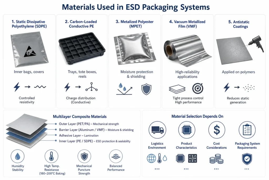
Materials Used in ESD Packaging Systems
ESD packaging materials consist of engineered composites, which are carefully selected based on their unique properties (e.g. electrical, mechanical and thermal) to meet specific needs. Examples of commonly used materials in ESD packaging include:
- Static dissipative polyethylene (SDPE) – a flexible film with controlled resistivity, used for inner bags and covers.
- Carbon-loaded conductive polyethylene – used for trays, tote boxes, and component reels where charge distribution is needed.
- Metalized polyester (MPET) – A thin aluminum layer is deposited on a PET film so that it can provide moisture protection and shielding. I often use polyethylene, which means it is usually used in multilayer foil packaging bags.
- Vacuum metallized film (VMF) – similar to MPET but with tighter process control, often used for high-reliability applications.
- Antistatic coatings – topical coatings applied directly to polymers to decrease generation of static electricity (though generally not as durable as built-in dissipative products).
Multilayer composite materials are developed by combining materials into advanced package systems that provide balanced performance characteristics of humidity stability, high temperature resistance (baking up to temperatures of approximately 180 – 200 degrees celcius) and mechanical puncture strength. Material selection will vary according to the attributes of the packaging system in relation to the particular logistics environment, the characteristics of the product being packaged, and costs considerations.
Manufacturing and International Standards
ESD packaging manufacture is a controlled polymer engineering process. Key steps include:
- Polymer compounding – Mixing Carbon black, carbon nanotubes, graphene or conductive fillers with the base resin or adding antistatic additives to base resin.
- Extrusion under controlled humidity – ensuring consistent dispersion and surface properties.
- Metallization or coating – depositing thin metal layers via vacuum evaporation or sputtering.
- Multilayer lamination – combining functional layers with adhesives to maintain integrity under flexing and heat.
- Heat sealing and forming – converting film into bags, pouches, or rigid trays.
All ESD packaging should comply with established international standards:
| قياسي | Scope |
|---|---|
| IEC 61340-5-1 | Electrostatic control systems for electronics; the global reference |
| ANSI/ESD S20.20 | ESD control program requirements; widely adopted in North America |
| IPC-1601 | PCB handling and storage guidelines; covers ESD packaging as part of process control |
| RoHS | Restriction of hazardous substances; environmental compliance |
Industry Insight: Over 80% of tier-1 electronics manufacturing service (EMS) providers require their packaging suppliers to hold certification for both IEC 61340-5-1 and ANSI/ESD S20.20 to ensure global compliance.
ESD Packaging in PCB Supply Chains
Electronic discharge (ESD) risks extend beyond just factories. Electrical discharges (ESD) pose a risk across the entirety of the worldwide logistics chain. The amount of risk associated with electrical discharges (ESD) is dependent on one’s location.
| Environment | Risk Level | Main Source | Recommended Packaging |
|---|---|---|---|
| SMT Production Line | عالٍ | Machine friction, operator handling | Multilayer shielding bags or bins |
| Air Freight | Very High | Low humidity (can fall below 10% RH at altitude) | Metallized shielding film with moisture barrier |
| Warehouse Storage | Medium | Charge accumulation on surfaces | Dissipative bags or covers |
| Cleanroom | عالٍ | Human contact, synthetic garments | Full ESD-protective packaging (bags, boxes, labels) |
| Ocean Shipping | Medium | Temperature and humidity cycles | Moisture-stable composite materials |
Air freight purchasers should request metallized shielding film with shielding effectiveness higher than 40 dB and also have a built-in moisture barrier. Because there is a very low level of humidity and there is a rapid pressure drop while climbing in altitude, there is an additional potential for generating ESD in the air freight environment.
Procurement Guide for ESD Packaging
Choosing a suitable ESD packaging supplier cannot be accomplished solely based on price; engineering performance is another factor to consider. When conducting the technical audit, the following criteria can be included:
- IEC / ANSI compliance certification – verified by an independent third-party (SGS, TÜV, etc.).
- Shielding effectiveness data – measured per IEC 61340-5-1 or ANSI/ESD STM11.31.
- Charge decay test reports – showing < 2 seconds decay time under stated temperature and humidity conditions.
- Humidity and temperature stability – performance curves across the expected logistics range (e.g., 20%–80% RH).
- OEM/ODM capability – ability to custom-design packaging geometry, material selection, and printing.
- Batch-to-batch consistency – internal quality control data showing CPK values above 1.33 for key parameters.
Industry Insight: Cost-driven selection of ESD packaging—without engineering validation—has been directly linked to a 5–8% increase in field failure rates among semiconductor packagers. Leading companies now require incoming quality control (IQC) testing on every lot.
أسئلة متكررة
Q1: What is ESD packaging for PCB used for?
Q2: Do PCBs really need ESD packaging?
Q3: Why do PCBs still fail after ESD packaging?
Q4: What is the best packaging for PCB shipping?
Q5: What should buyers check before choosing suppliers?
Q6: Can standard pink‑poly antistatic bags provide adequate protection?
Q7: How often should ESD packaging be requalified?
Q8: Is there a difference between “static dissipative” and “conductive” packaging?
ESD packaging for PCB manufacturers is a technical discipline grounded in electrical engineering, materials science, and standards compliance. It is not an accessory—it is a critical component of the overall reliability assurance system for electronic products. From understanding failure mechanisms and multilayer design principles to selecting materials and qualifying suppliers against IEC and ANSI standards, every decision matters.
For procurement and engineering teams, the takeaway is clear: treat ESD packaging as an engineered reliability solution, not a commodity. Invest in supplier verification, performance testing, and logistics-specific design. The cost of doing so is small compared to the field failure exposure that latent ESD damage can cause—especially in automotive, aerospace, and industrial applications where reliability is paramount.
By applying the principles and data outlined in this guide, buyers and engineers can significantly reduce ESD-related risks and build a more resilient electronics supply chain.
المراجع
- IEC 61340-5-1: Electrostatic Control Standard – International Electrotechnical Commission. https://webstore.iec.ch/en/publication/74748
- ANSI/ESD S20.20: ESD Control Program Standard – EOS/ESD Association. https://www.esda.org
- IPC-1601: PCB Handling and Storage Guidelines – IPC. https://www.ipc.org
- EOS/ESD Association Technical Publications. https://www.esda.org
- MarketsandMarkets. “Electronics Packaging Market Report” (2023). https://www.marketsandmarkets.com


اترك ردًا